


OPA387 Zero-Drift Op Amp: 7 Checks for Microvolt Errors and Switching Artifacts

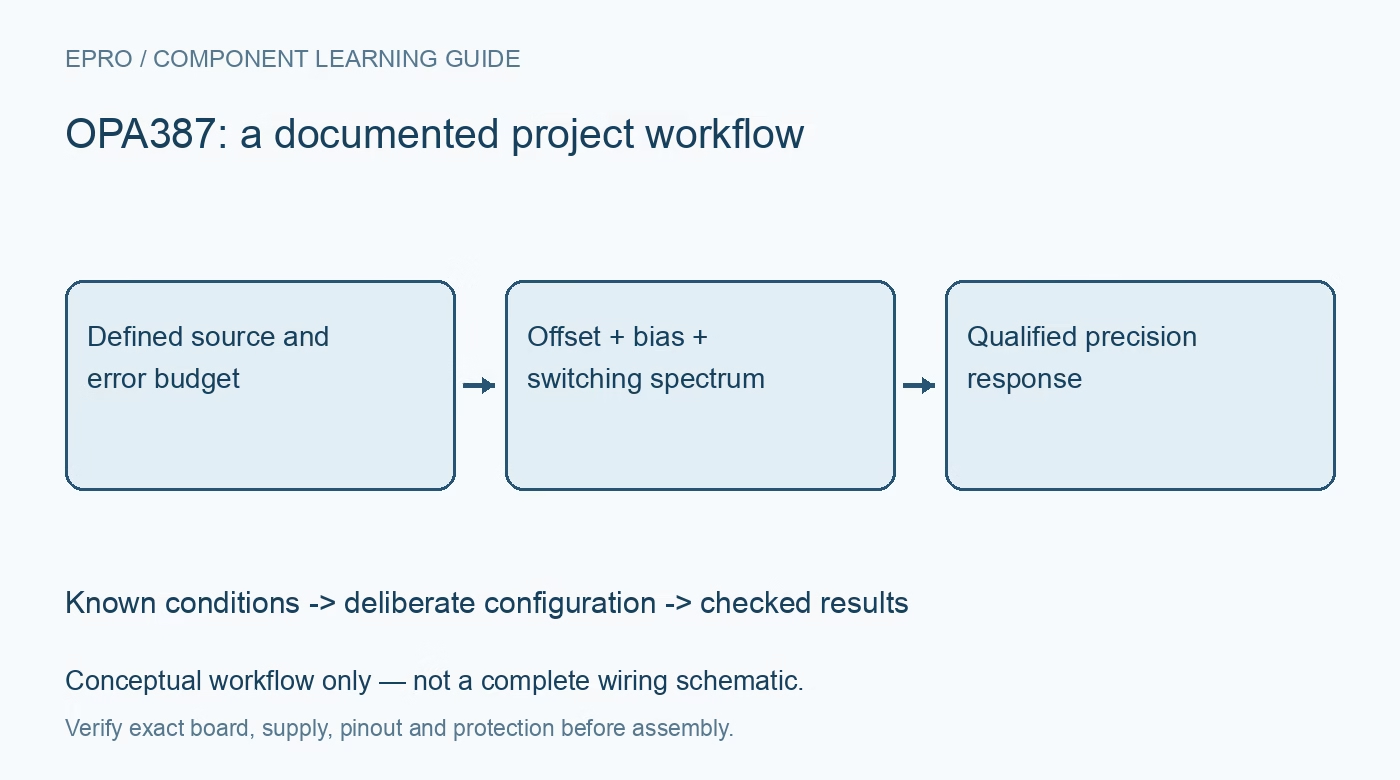
OPA387 Zero-Drift Op Amp: 7 Checks for Microvolt Errors and Switching Artifacts
Build an OPA387 error budget covering supply-dependent offset limits, bias current, thermal EMFs, chopping artifacts and settling conditions. This is a documentation-based planning guide, not a report of independent hands-on testing.
1. Define the actual precision target and supply
The OPA387 is a zero-drift amplifier operating from 1.7 to 5.5 volts total supply. Describe the input span, required gain, source resistance, output load and acceptable input-referred error before choosing surrounding components. Rail-to-rail terminology does not eliminate common-mode or output-swing conditions. Check the electrical table for the intended supply and load. A very small offset specification does not by itself make a circuit an accurate twenty-four-bit measurement system, particularly when the reference, resistors and ADC have separate errors. Manufacturer documentation.
2. Keep offset limits tied to their test conditions
The electrical table lists a two-microvolt maximum offset at a 5.5-volt supply under the stated test conditions, but 2.5 microvolts at 1.7 volts. Do not turn the more attractive number into a universal bound. Likewise, the OPA387 typical drift of 0.003 microvolts per degree Celsius is not its maximum drift specification. Use appropriate limits for the error budget and keep typical values labeled. Include gain error and resistor-ratio drift separately instead of attributing the entire circuit accuracy to amplifier offset. Manufacturer documentation.
3. Translate bias current through real source impedance
OPA387 input bias current has a 150-picoamp maximum at the stated room-temperature test conditions, not the femtoamp specification of a different amplifier. An illustrative one-megohm unmatched source resistance multiplied by 150 picoamps produces 150 microvolts, already much larger than the offset headline. That calculation is not a complete worst-case model across temperature, but it exposes an important design risk. Budget input-current mismatch, source imbalance and board leakage, then evaluate whether a lower impedance or different topology is appropriate. Manufacturer documentation.
4. Treat thermal junctions and contamination as circuit elements
At microvolt levels, temperature gradients across dissimilar-metal junctions can create unwanted thermoelectric voltages. Keep sensitive input paths physically balanced and away from warm regulators, connectors and airflow changes. Cleanliness and humidity also matter when source impedances are high. Define how the measurement will settle after handling the board. An apparently drifting zero can come from external thermal or leakage effects even when the amplifier meets its specifications. Document these mechanisms rather than promising that zero-drift technology eliminates all calibration needs. Manufacturer documentation.
Newest in the store


5. Check switching artifacts against the sampling bandwidth
The offset-cancellation architecture switches internally. The electrical table gives a minimum chopping frequency of 100 kilohertz and a typical value of 150 kilohertz; 150 kilohertz is not a guaranteed upper limit or a universal fixed clock. Consider how residual switching-related content, input filtering and ADC sampling can interact. A low-frequency signal of interest does not automatically prevent higher-frequency components from aliasing into its measurement band. Inspect the relevant noise and filtering guidance, then validate the complete signal chain. Do not invent a guaranteed ripple amplitude or filter rejection from the architecture label alone. Manufacturer documentation.
6. Distinguish bandwidth, settling and overload recovery
Small-signal bandwidth does not specify settling to a precision error band after every possible step. The table gives a 5.5-microsecond settling example to 0.01 percent for a one-volt step at unity gain under its stated conditions. Output capacitance, gain, driver loading and source behavior can change the real result. TI also warns that large differential input separation can disturb the internal offset-cancellation path and produce extended settling. Avoid saturating the amplifier during qualification and then interpreting its recovery as ordinary linear response. Manufacturer documentation.
7. Validate a complete low-voltage precision record
Record supplies, gain network, source impedances, filtering, ADC timing, load and thermal conditions. Begin with a controlled zero input and several bounded reference levels, then compare noise and error against the intended budget. Mark values measured on the actual board separately from datasheet limits and calculations. Include startup, a realistic step and a settling interval before accepting readings. The useful outcome is a defensible measurement uncertainty with known conditions, not a blanket claim that low offset guarantees every digit displayed by the software. Manufacturer documentation.
Related reading: OPA392 Precision Op Amp: 7 Checks for Noise Bandwidth and ADC Settling.
Catalog note: The exact-part search did not return a matching Epro listing during preparation. Check the current catalog; this guide makes no price, availability or included-accessory claim.