


ADS8860 SAR ADC: 7 Checks for Reference and Busy Modes

ADS8860 SAR ADC: 7 Checks for Reference and Busy Modes
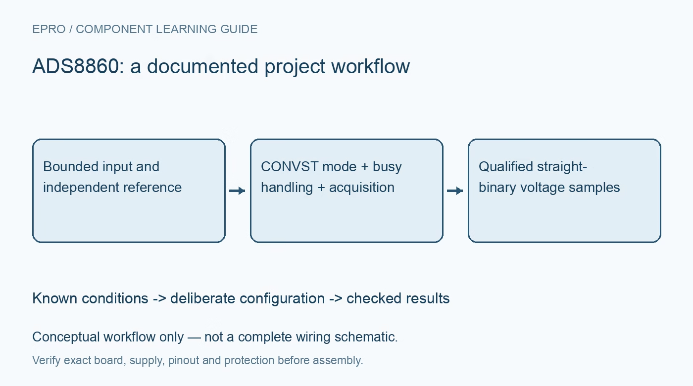
Plan ADS8860 sampling with seven checks for independent reference voltage, near-ground AINN, CONVST mode selection, busy framing and acquisition. This is a documentation-based planning guide, not a report of independent hands-on testing.
1. Separate the three voltage domains
ADS8860 is a sixteen-bit, up-to-1-MSPS SAR converter. AVDD operates from 2.7 V to 3.6 V, DVDD from 1.65 V to 3.6 V, and the external reference from 2.5 V to 5 V under documented conditions. The reference may exceed AVDD; that is an intentional feature, not permission to apply 5 V to the supply or digital pins. Review the complete pin ratings, host thresholds and sequencing before assembly, including what happens if one voltage domain is absent. Manufacturer documentation.
2. Keep the negative input close to ground
Although two input pins are sampled, this is a single-ended unipolar converter, not a full-range differential ADC. AINN is restricted to a small range around ground, while AINP follows the permitted reference-related input range. The ideal signal range is zero to VREF. Do not connect an arbitrary floating differential source on the assumption that both pins can swing through the full scale. Protect the inputs and begin with known low-voltage levels inside the recommended limits. Manufacturer documentation.
3. Drive REF for dynamic conversion current
The reference pin sees switched-capacitor loading during conversion. A reference source with an accurate unloaded DC voltage can still produce distortion or code error if it cannot supply the dynamic charge. Follow the manufacturer reference-driver and bypass guidance, accounting for buffer stability and effective capacitor value. Measure reference behavior with an appropriate technique rather than adding long probe leads to a sensitive node. Document the actual reference voltage because it sets the code-to-voltage conversion independently of the analog supply. Manufacturer documentation.
4. Select the interface using DIN at the sampling edge
A rising CONVST edge samples the input and begins conversion. DIN high at that edge selects CS mode; DIN low, or DIN connected to CONVST in the documented arrangement, selects daisy-chain operation. DIN is therefore not merely an ignored serial input. Choose one supported interface and implement its full timing diagram. A reset or GPIO initialization that leaves DIN in the wrong state can alter framing even though the host still receives changing bits. Manufacturer documentation.
Newest in the store




5. Decide explicitly whether a busy indicator is present
CS and chain interfaces have documented versions with and without a busy indication. Its generation depends on control-signal levels at conversion completion, and busy-enabled operation adds a marker ahead of conversion data. Do not silently decode every receive buffer as sixteen data bits beginning at the same position. Check the required pull-up, receive-clock count and release timing for the selected mode. Begin with a single device and fixed input levels before adding interrupts, shared buses or chains. Manufacturer documentation.
6. Allocate conversion and acquisition time separately
Conversion uses an internal clock with bounded minimum and maximum duration; SCLK is for reading data, not driving the conversion engine. The result is read after conversion while the converter acquires the next sample. Reserve enough acquisition time for source impedance, input network and worst-case voltage steps, not just enough serial clocks to empty the output word. The maximum sample-rate headline assumes a suitable driver and timing budget. Reducing throughput can help settling but does not automatically solve a poor reference or unstable amplifier. Manufacturer documentation.
7. Validate raw framing before scaling to volts
Output is straight binary: ideal midscale is 0x8000, not signed zero, and an ideal step is VREF divided by 65536. Verify zero-region, midscale and high-range inputs while staying within all input limits. Log raw frames, selected mode, busy interpretation, CONVST timing and reference voltage with each sample set. Test large allowed steps and reset recovery to expose stale or misaligned data. Only convert to an engineering value after both framing and settling have been demonstrated for the intended operating conditions. Manufacturer documentation.
Related reading: ADS8866 SAR ADC: 7 Checks for CONVST Mode and Input Settling.
Catalog note: The exact-part search did not return a matching Epro listing during preparation. Check the current catalog; this guide makes no price, availability or included-accessory claim.