


DAC7512 Voltage DAC: 7 Checks for Supply Reference and Frames

DAC7512 Voltage DAC: 7 Checks for Supply Reference and Frames
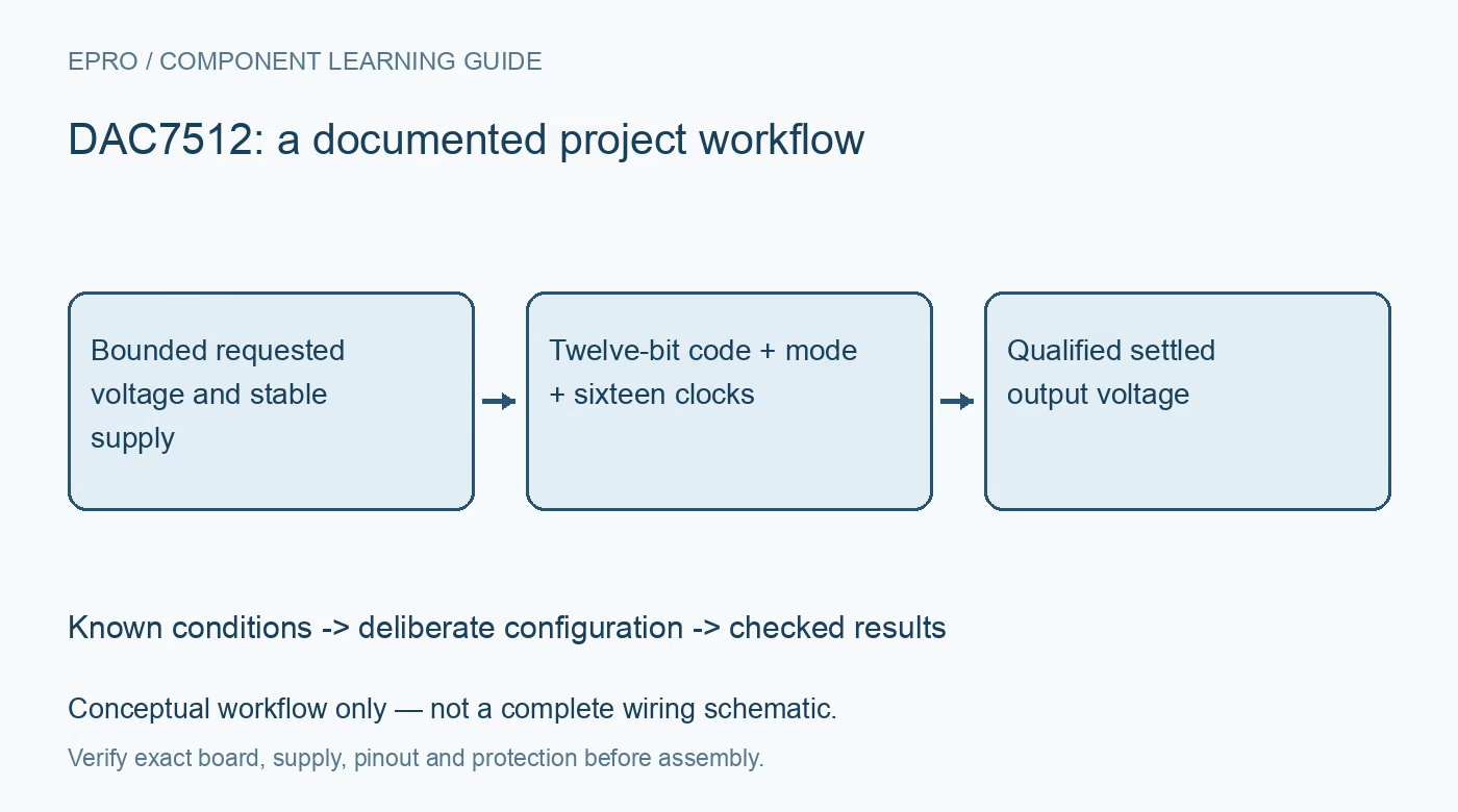
Plan DAC7512 outputs with seven checks for the supply-derived reference, 16-bit frames, power-down fields, SYNC timing and output settling. This is a documentation-based planning guide, not a report of independent hands-on testing.
1. Identify what the supply does in this DAC
DAC7512 is a single twelve-bit buffered voltage-output DAC operating from 2.7 V to 5.5 V. Its supply is also the conversion reference: there is no independent external-reference pin to wire or internal-reference command to enable. Check the exact six-pin package drawing before connecting serial signals and output. This makes supply accuracy and noise part of the voltage-setting problem rather than a secondary power detail. A numerically correct command cannot compensate automatically for an unmeasured or drifting supply. Manufacturer documentation.
2. Convert requested voltage into a bounded twelve-bit code
The ideal equation is VOUT = VDD multiplied by code divided by 4096. Code ranges from zero through 4095; the maximum code is one ideal step below the supply. With a 3.3-V supply, midscale ideally requests 1.65 V, and one step is approximately 0.806 mV. Real output depends on supply error, offset, gain, loading and headroom. Clamp requested codes deliberately and flag out-of-range voltages instead of allowing integer wraparound to produce an unrelated output. Manufacturer documentation.
3. Put control bits in the correct sixteen-bit frame
The serial word contains two leading don’t-care bits, then PD1 and PD0, followed by twelve data bits. Normal operation requires both power-down bits low. Accidentally shifting a twelve-bit value into the wrong position can therefore select a different operating mode rather than merely scale the output incorrectly. Build the frame from named masks and verify known test patterns. A library for another similarly named DAC may assume a different word length, channel field or reference behavior. Manufacturer documentation.
4. Understand when the output command actually takes effect
Bring SYNC low and shift the complete word on falling SCLK edges. The selected action occurs on the sixteenth falling edge, not on the later SYNC rising edge. Raising SYNC before the complete frame aborts the write without updating the output. Before another command, SYNC must go high for the specified minimum interval; the documentation gives 33 nanoseconds. Capture the real waveform and respect timing at the selected supply rather than inferring a valid transaction from the SPI software return code. Manufacturer documentation.
Newest in the store


5. Separate SPI throughput from analog settling
A fast serial clock can deliver a command much sooner than the output settles. The documentation gives an unloaded half-scale settling example of about 8 microseconds, with output behavior dependent on the applied step and load. That example is not a universal update-rate guarantee. Measure after a justified settling interval, and check representative low, middle and high transitions. A waveform generator built around the DAC must budget both command timing and analog settling, including any external filter or buffer. Manufacturer documentation.
6. Distinguish reset zero from the three power-down states
Power-on reset initializes the output code to zero until a valid command is received. Power-down instead selects a typical 1-kilohm connection to ground, 100-kilohm connection to ground or high-impedance output, according to the two control bits. These states have different implications for a downstream load or externally biased node. Recovery also has a finite documented time. Define the application-safe state explicitly, and do not call a high-impedance output zero volts simply because the converter is consuming little current. Manufacturer documentation.
7. Validate the reference and output in the same record
Start with a high-impedance measurement load and a current-limited, clean supply. Record VDD at the device alongside command bytes, measured VOUT, load and elapsed settling time. Compare a bounded sequence of codes, then repeat under the intended supply and load conditions to separate reference movement from DAC error. Check reset and power-down recovery before attaching sensitive downstream electronics. The final result should be a reproducible command-to-voltage relationship for stated conditions, not a precision claim based solely on twelve-bit resolution. Manufacturer documentation.
Related reading: DAC8551 Voltage DAC: 7 Checks for Feedback and Serial Updates.
Catalog note: The exact-part search did not return a matching Epro listing during preparation. Check the current catalog; this guide makes no price, availability or included-accessory claim.