


Advantages of Using smd components

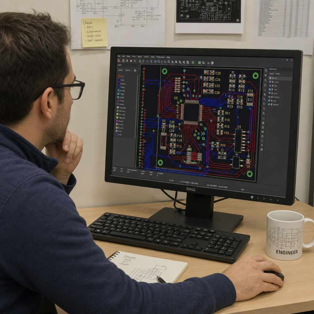
Advantages of Using smd components
SMD components are a practical choice for modern electronics because they support compact layouts, efficient production, and reliable performance when the design and assembly process are handled correctly. Whether you are developing a consumer device, industrial controller, lighting product, sensor module, or communication board, surface mount technology can help turn a cleaner design into a more manufacturable product. This guide explains how SMD parts work, why they are widely used, and what to consider before choosing them for your next surface mount circuit.
What is a surface mount device?
A surface mount device is an electronic component designed to be mounted directly onto the surface of a printed circuit board rather than inserted through drilled holes. If you have ever searched “what is a surface mount device” or “what is surface mount device,” the simplest answer is this: it is a component built for surface-level placement, automated assembly, and compact electronic design.
Unlike traditional through-hole components, SMD parts do not usually have long wire leads that pass through the board. Instead, they use small metal pads, terminals, or end caps that connect to matching pads on the PCB. During surface mount assembly, solder paste is applied to those PCB pads, the parts are positioned on top, and the board is heated so the solder forms secure electrical and mechanical connections.
That difference may sound small, but it changes how a product is designed and manufactured. SMD components can be placed on one or both sides of a board, they take up less space, and they are well suited to automated pick-and-place equipment. This is one reason surface mount technology has become the standard for many high-volume and space-sensitive electronics.

Surface mount technology makes compact electronics easier to build
One of the biggest advantages of SMD components is space efficiency. Because the parts sit directly on the board surface, they typically require less PCB area than through-hole equivalents. Designers can place resistors, capacitors, ICs, diodes, sensors, and a surface mount device LED in tighter arrangements, creating smaller boards without sacrificing core functionality.
This matters in real-world products. Wearable devices, handheld tools, LED lighting modules, smart home controls, medical accessories, automotive electronics, and wireless sensors all benefit from smaller and lighter assemblies. A compact surface mount design can reduce enclosure size, lower material use, and make room for batteries, antennas, connectors, displays, or mechanical features.
Surface mount technology also gives engineers more layout flexibility. Since there are fewer drilled holes competing for routing space, traces can often be arranged more efficiently. In multilayer boards, this can support cleaner signal paths and more practical power distribution. The result is not simply a smaller board, but a board that may be easier to optimize for performance, manufacturability, and product packaging.
The space-saving benefit becomes even more valuable when a design must include many passive parts. A circuit that uses dozens or hundreds of resistors and capacitors can become bulky with through-hole components. With SMD components, the same functional circuit can often be made far more compact, which is why SMD manufacturing is closely associated with modern electronics miniaturization.
The practical advantages of SMD components
SMD components are popular because they solve several design and production challenges at once. They are not automatically the best choice for every circuit, but for many applications, their benefits are significant.
Key advantages include:
- Smaller board footprint: SMD parts help reduce PCB size and make dense layouts possible.
- Lower assembly labor: Automated placement can reduce the need for manual component insertion.
- Good fit for volume production: Surface mount assembly works well when repeatability and speed matter.
- Two-sided placement options: Components can often be mounted on both sides of the PCB when the design allows it.
- Reduced drilling requirements: Fewer through-holes can simplify PCB fabrication and preserve routing space.
- Shorter electrical paths: Small packages and close placement can support cleaner layouts in many circuits.
- Wide component availability: Many modern ICs, passives, LEDs, and modules are primarily offered in SMD packages.
These benefits often work together. For example, a smaller footprint may allow a designer to reduce board size, but it may also improve enclosure fit and simplify final product assembly. Automated placement may support faster production, but it also improves consistency when compared with placing many tiny parts by hand.
Another advantage is design scalability. A prototype built with SMD components can often move more naturally toward production than a prototype built entirely with oversized through-hole substitutes. This does not mean every prototype must use the final smallest package, but it does mean that considering SMD early can prevent redesign work later.
SMD components can also support better visual organization on the board. When footprints, reference designators, and placement rules are planned carefully, the finished PCB can be easier to inspect, test, and document. That practical clarity matters when multiple teams are involved in engineering, purchasing, production, and quality control.
SMD vs through-hole: which option fits your project?
The choice between SMD vs through-hole depends on the product, production volume, mechanical requirements, repair needs, and available assembly process. SMD is often preferred for compact, automated, and high-density electronics, while through-hole remains useful for parts that need strong mechanical anchoring or easy manual handling.
Through-hole components still have an important place. Connectors, large capacitors, relays, transformers, terminal blocks, high-stress switches, and some power components may benefit from leads that pass through the board. If a component will be pulled, pushed, twisted, or exposed to frequent mechanical stress, through-hole mounting may provide useful strength.
SMD components are usually better when board space is limited, production will be automated, or the circuit uses many small passives and ICs. They also make sense when the component package is only available in surface mount form, which is increasingly common for advanced semiconductors and miniature devices.
A balanced design may use both methods. Many boards combine SMD resistors, capacitors, LEDs, and integrated circuits with through-hole connectors or high-power parts. This hybrid approach lets designers use surface mount technology where it provides efficiency while keeping through-hole components where mechanical durability or serviceability is more important.
When comparing the two, ask practical questions:
- How small does the final product need to be? If size is critical, SMD components usually have the advantage.
- Will the board be assembled by machine or by hand? Automated assembly strongly favors SMD, while hand assembly may favor larger packages or through-hole parts.
- Does the component need mechanical strength? Through-hole may be better for heavily stressed components.
- Will technicians need to repair or replace parts easily? Larger through-hole components and larger SMD packages are often easier to service.
- What packages are available from suppliers? Some parts may only be practical or readily available as surface mount device packages.
The best decision is rarely based on one factor. A good surface mount design balances electrical needs, mechanical constraints, manufacturing realities, sourcing availability, and long-term support.

Better manufacturability starts with thoughtful surface mount design
Using SMD components successfully begins before assembly. The PCB layout, component selection, pad geometry, spacing, orientation, and thermal planning all influence how well the final board can be manufactured. A design that looks correct schematically may still create production issues if it is difficult to place, solder, inspect, or test.
A strong surface mount design starts with appropriate package selection. Very small components can save space, but they may also increase placement sensitivity, inspection difficulty, and rework complexity. For many products, the smallest possible package is not automatically the best choice. Designers often choose a package that balances density with reliable assembly and practical sourcing.
Footprint accuracy is equally important. The PCB land pattern must match the component package and the assembly process. Pads that are too large, too small, uneven, or poorly spaced can contribute to solder defects. Good libraries, verified footprints, and careful design reviews help reduce avoidable errors.
Thermal behavior also deserves attention. Some SMD components dissipate heat through pads connected to copper areas or thermal vias. If the layout does not provide a reasonable heat path, the part may run hotter than expected. For LEDs, regulators, power ICs, and drivers, thermal design is not an afterthought; it is part of the component selection and PCB layout process.
Useful design practices include:
- Keep component orientation consistent where practical to support assembly and inspection.
- Leave enough spacing for pick-and-place nozzles, solder joints, and inspection access.
- Use manufacturer-recommended footprints when available, then adapt only with clear reason.
- Consider test points early, especially for programming, debugging, and production testing.
- Avoid placing heat-sensitive parts too close to hot components without reviewing thermal impact.
- Think about rework access if the product may require repair, tuning, or engineering changes.
Good SMD design is practical design. It supports the electrical function of the circuit while also helping the manufacturer build the board repeatedly and efficiently.
SMD soldering and assembly require process control
SMD soldering is different from traditional hand soldering because the process usually depends on solder paste, accurate placement, and controlled heating. In production, solder paste is commonly printed onto the board through a stencil. Components are then placed onto the paste, and the board passes through a reflow process that melts and solidifies the solder.
This workflow supports repeatability, but it also requires control. Paste volume, stencil quality, component alignment, reflow profile, board finish, and package type can all influence solder joint quality. If one part of the process is poorly matched to the design, defects can appear even when the circuit itself is correct.
Common SMD soldering concerns include insufficient solder, excess solder, tombstoning of small passive components, solder bridging between fine-pitch leads, and poor wetting. Many of these issues can be reduced through good footprint design, proper stencil openings, balanced pad geometry, and stable process settings.Newest in the store


Hand soldering is still possible for many SMD components, especially larger packages. Engineers and technicians often hand-solder SMD parts during prototyping, repair, or modification. However, very small packages, fine-pitch ICs, and bottom-terminated components can be challenging without the right tools and experience.
For a smoother surface mount assembly process, teams should prepare clear manufacturing data. That typically includes accurate Gerber files, a complete bill of materials, centroid or pick-and-place data, assembly drawings, polarity markings, and any special notes for sensitive components. Clear documentation reduces back-and-forth, helps purchasing confirm parts, and gives the assembler what they need to build the board correctly.
SMD components support modern LED and lighting applications
A surface mount device LED is a good example of how SMD packaging can improve product design. SMD LEDs are widely used because they are compact, efficient to place, and available in many colors, brightness levels, viewing angles, and package styles. They can be used for indicators, displays, backlighting, light strips, control panels, signage, and general lighting modules.
In lighting products, compact size is only one advantage. SMD LEDs can be arranged in dense patterns to create even illumination, flexible layouts, or specialized light distribution. This gives designers more freedom when developing slim fixtures, illuminated interfaces, decorative lighting, and compact electronic indicators.
Thermal management remains important. LEDs are sensitive to heat, and the PCB must help move heat away from the device when power levels require it. Copper area, board material, current control, spacing, and enclosure ventilation can all affect long-term performance. A well-designed LED surface mount circuit considers both electrical drive conditions and heat dissipation.
SMD LEDs also highlight the importance of polarity and orientation. Assembly drawings and silkscreen markings should make LED direction clear to prevent placement errors. When boards include many LEDs, consistency in orientation can speed inspection and reduce confusion during production.
A reliable sourcing plan protects the build
Component sourcing is a major part of any electronics project. Even the best design can run into delays if parts are hard to find, poorly documented, or purchased from unreliable channels. Working with a reputable surface mount device distributor can help teams access suitable parts, confirm package details, and manage availability more effectively.
For production planning, it is useful to identify approved alternatives where possible. A resistor or capacitor may have several acceptable substitutes, while a microcontroller, sensor, LED, or power IC may require tighter approval. The bill of materials should clearly define what can be substituted and what cannot.
Surface mount device distributors can also support purchasing teams by helping verify manufacturer part numbers, packaging formats, minimum order quantities, and lifecycle status. This is especially important when the assembly process requires tape-and-reel packaging for automated placement. A part may be electrically correct but inconvenient for production if it is only available in a format that slows assembly.
Some buyers look for a surface mount device stocking manufacturer or stocking supplier model when they need faster access to frequently used components. The goal is not simply to find parts, but to reduce sourcing risk. For recurring builds, stable access to approved SMD components can be just as important as the PCB layout itself.
A practical sourcing checklist includes:
- Confirm the exact manufacturer part number and package.
- Check whether the part is available in production-friendly packaging.
- Review datasheets for dimensions, land pattern guidance, polarity, and thermal notes.
- Identify acceptable alternates before a shortage forces a rushed decision.
- Keep engineering, purchasing, and assembly teams aligned on approved substitutions.
- Avoid changing a component without checking electrical, mechanical, and process impact.
Good sourcing protects schedule, quality, and repeatability. It also helps prevent last-minute redesigns caused by unavailable or mismatched parts.
SMD manufacturing improves repeatability when the design is ready
SMD manufacturing is built around repeatable process steps. Once the PCB design, stencil, placement data, component reels, and reflow profile are prepared, the same operation can be repeated across many boards with consistent results. That repeatability is one reason SMD is so valuable for commercial electronics.
Automation does not remove the need for engineering judgment. It simply makes preparation more important. A misplaced polarity mark, unclear BOM entry, incorrect footprint, or incomplete assembly note can create repeated errors quickly. The stronger the design package, the better the manufacturing process can perform.
Inspection is another important part of SMD manufacturing. Visual inspection, automated optical inspection, and electrical testing can help identify solder defects, missing parts, reversed components, or assembly issues. The right inspection method depends on board complexity, component type, production volume, and product requirements.
Designers can make inspection easier by using clear reference designators, accessible test points, logical component orientation, and adequate spacing around critical parts. These details may seem small during layout, but they become valuable when a board must be built, checked, diagnosed, and improved.
SMD manufacturing also supports product consistency. When parts are placed by automated equipment and soldered through a controlled process, variation from board to board can be reduced. For businesses moving from prototype to production, that consistency helps create a more predictable path from engineering validation to repeat builds.
When SMD components may not be the best fit
SMD components offer many benefits, but they are not ideal for every situation. Some projects are better served by through-hole parts, larger packages, or a mixed assembly method. Recognizing these limits helps avoid design choices that create unnecessary manufacturing or service challenges.
SMD may be less suitable when a part needs exceptional mechanical strength, when the assembly will be performed entirely by beginners using basic hand tools, or when field repair is a major priority. Very small SMD packages can also be difficult to inspect or replace without magnification, hot air tools, and steady technique.
High-power designs require extra care as well. Many power components are available in SMD packages, but the board must be designed to handle heat and current properly. Copper weight, trace width, thermal pads, vias, airflow, and enclosure conditions can affect reliability. Choosing SMD for power applications is common, but it must be done with careful layout and thermal planning.
There are also learning curve considerations. Teams new to surface mount assembly may need time to develop good library management, stencil practices, reflow setup, inspection standards, and rework skills. Starting with moderately sized SMD packages can make early projects more manageable before moving into ultra-miniature components.
Practical tips for getting better results with SMD components
A successful SMD project is the result of many good small decisions. Component selection, PCB layout, documentation, sourcing, and assembly planning all affect the final outcome. Treating these areas as connected instead of separate can reduce errors and improve production readiness.
Use this checklist before sending a surface mount circuit to fabrication or assembly:
- Review the schematic and BOM together. Make sure every selected part matches the electrical requirements and package assumptions.
- Verify all footprints. Compare land patterns against datasheets, especially for ICs, LEDs, connectors, and polarized parts.
- Check component spacing. Leave enough room for assembly, inspection, heat management, and potential rework.
- Confirm polarity markings. Diodes, LEDs, electrolytic capacitors, ICs, and connectors should be clearly marked.
- Plan for test access. Add test points for important signals, power rails, programming lines, and ground.
- Coordinate with the assembler early. Ask about preferred design rules, stencil considerations, and file requirements.
- Validate sourcing before layout is final. Make sure critical components are available from suitable suppliers.
- Build and inspect prototypes carefully. Use prototype feedback to refine the layout before committing to larger production.
These steps are not complicated, but they are easy to overlook under schedule pressure. A little extra review before manufacturing can save time later, especially when a design uses fine-pitch parts or dense placement.

SMD components are a foundation for modern electronics
SMD components help make electronics smaller, cleaner, and more production-ready. They support compact layouts, automated assembly, broad component selection, and efficient use of PCB space. For many products, surface mount technology is not just an alternative to through-hole construction; it is the practical foundation of the design.
The best results come from matching the technology to the application. Use SMD where compact size, repeatable assembly, and layout flexibility matter. Use through-hole where mechanical strength, simple hand assembly, or easy service access is more important. Many strong designs use both.
If you are planning a new board, think beyond the individual component. Consider the complete path from surface mount design to sourcing, SMD soldering, surface mount assembly, inspection, and future builds. When these decisions work together, SMD components can help create electronics that are not only smaller, but also easier to manufacture, scale, and support.