


OPA333 Zero-Drift Op Amp: 7 Checks for a Quiet DC Signal Path

OPA333 Zero-Drift Op Amp: 7 Checks for a Quiet DC Signal Path
Plan an OPA333 DC signal path with explicit feedback, bias return, output headroom, settling and ADC loading rather than assuming zero drift means zero error. This is a documentation-based planning guide, not a report of independent hands-on testing.
1. Identify the amplifier topology you actually need
OPA333 is a single operational amplifier; OPA2333 is the dual version. Neither name should be confused with INA333, an instrumentation amplifier with a different gain architecture. Draw the intended feedback circuit, source impedance and output load before calculating gain. A differential sensor does not automatically become an instrumentation-amplifier application by connecting two pins to an op amp. Choose a topology that satisfies common-mode rejection, bias-return and input-range requirements for the actual signal source. Manufacturer documentation.
2. Build an error budget beyond offset voltage
Zero-drift describes the amplifier’s offset-correction approach, not zero total error. Separate input offset, drift, input bias effects, resistor ratio error, noise and reference uncertainty. For a high-impedance source, even small bias currents can create a meaningful voltage error. Use maximum or typical figures according to the requirement and stated test conditions. Refer each contribution to the appropriate input or output node before combining it, and avoid treating a low typical offset as a guaranteed complete-system accuracy. Manufacturer documentation.
3. Check common-mode and output headroom separately
The device operates from a 1.8 V to 5.5 V total supply range, with rail-to-rail input and output capability subject to specified conditions. That wording does not mean every output reaches either rail exactly under any load. Check the input common-mode range, feedback demand and output-swing specification at the proposed current. Calculate the largest expected output including error and transient margin. A valid input can still demand an impossible output voltage once gain and reference offset are applied. Manufacturer documentation.
4. Provide feedback and a defined bias-current path
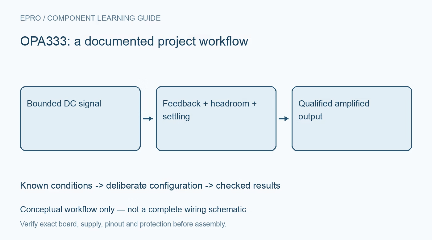
Verify feedback polarity, resistor values and the DC return path for every input. AC coupling or a floating sensor can otherwise leave the amplifier without a valid operating point. Keep sensitive nodes clean and route them away from leakage sources and switching traces. Include source resistance in the noise and bias analysis. Before connecting the final sensor, use a bounded known source to confirm closed-loop behavior; an output at a rail is not evidence of useful amplification. Manufacturer documentation.
Newest in the store


5. Budget bandwidth and settling for the real signal
The amplifier’s low-power precision role does not make it an unlimited-speed buffer. Evaluate closed-loop bandwidth, slew demands and settling using the documented behavior and the chosen noise gain. Startup also requires time for the specified offset performance to be established. Do not combine the first sample after power application with a steady-state accuracy claim. For changing inputs, distinguish a slowly moving real signal from the amplifier’s own recovery, filtering or saturation behavior before reporting a measurement. Manufacturer documentation.
6. Check ADC loading and capacitive stability
A sampled ADC input can draw short charge pulses even when its average current is small. Evaluate whether the amplifier, any isolation resistor and the local capacitor can settle within the ADC acquisition interval. Adding an arbitrary large capacitor directly to the output is not a universal noise fix; assess stability and transient response using the applicable guidance. Observe the output under the real acquisition pattern, not only with a high-impedance meter while the converter is idle. Manufacturer documentation.
7. Record repeatable DC qualification evidence
Measure known input points after appropriate stabilization, then examine output error, noise and settling under the intended load. Save supply voltage, gain components, source resistance, reference level, temperature conditions and sampling method. Keep offset-correction architecture distinct from a claim that the assembled board has no noise or drift. This is a documentation-based design checklist, not independent bench data. Revisit the budget whenever gain, ADC timing, supply arrangement or source impedance changes, even if the amplifier part number stays the same. Manufacturer documentation.
Related reading: INA333 Instrumentation Amplifier: 7 Checks Before Raising Gain.
Catalog note: The exact-part search did not return a matching Epro listing during preparation. Check the current catalog; this guide makes no price, availability or included-accessory claim.