


OPA827 JFET Op Amp: 7 Checks for Common-Mode Margin and Capacitive Loads

OPA827 JFET Op Amp: 7 Checks for Common-Mode Margin and Capacitive Loads
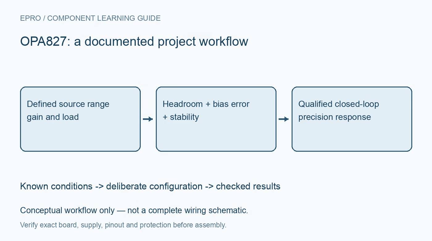
Plan OPA827 precision circuits with supported rails, non-rail-to-rail inputs, source-error budgets, capacitive-load limits and realistic settling. This is a documentation-based planning guide, not a report of independent hands-on testing.
1. Start with a supported supply arrangement
OPA827 is specified for the documented supply range corresponding to plus or minus 4V through plus or minus 18V. It is not a direct 3.3V or 5V controller-rail amplifier. Check the package pinout, local bypassing and signal reference before wiring a source. Use a bounded current-limited supply for initial tests. A precision-amplifier label does not remove the need to verify where the input and output voltages sit relative to the actual rails. Manufacturer documentation.
2. Reserve common-mode and output headroom
The input common-mode specification requires margin of approximately 3V from each supply rail under the listed conditions. It is not rail-to-rail. On plus-or-minus 5V supplies, that leaves roughly a minus-2V to plus-2V input window for that specification, not the full supply span. Check both amplifier inputs, including transitions and source faults. Output swing has its own load-dependent constraints. Keep those separate from common-mode limits when deciding gain, offset and maximum signal amplitude. Manufacturer documentation.
3. Translate JFET bias current into source error
Low input bias current is valuable for high-impedance sources, but it still produces error through source resistance. As a simple illustration, 10pA through 10 megohms gives 100 microvolts before other contributions. Use the applicable specification and temperature conditions rather than treating that calculation as a guaranteed board result. Connector leakage, contamination and humidity can dominate. Include resistor thermal noise and the source capacitance, since reducing DC loading does not automatically create a fast or low-noise signal path. Manufacturer documentation.
4. Keep bandwidth and slew requirements separate
The 22MHz gain-bandwidth and 28V-per-microsecond slew-rate figures describe different limitations. Estimate closed-loop bandwidth using noise gain and the relevant response curves, then check large-signal slope at the intended amplitude. For a sine wave, required slope is two pi times frequency times peak amplitude. A signal may lie below a small-signal bandwidth limit yet demand too much slew rate. Verify distortion and settling under the actual load instead of selecting the part from one frequency headline. Manufacturer documentation.
Newest in the store


5. Qualify the real capacitive load
The datasheet demonstrates substantial capacitive-load drive in specific buffer configurations, but also explains that load capacitance limits bandwidth and that gain and overshoot requirements matter. A successful manufacturer example is not a guarantee for every cable, capacitor dielectric or parallel load. Include output capacitance, ESR, wiring inductance and receiver behavior in the stability review. Inspect ringing and settling after representative steps. Add any isolation network through a deliberate design process rather than assuming more capacitance always improves noise without another cost. Manufacturer documentation.
6. Do not confuse phase protection with accuracy
Phase-reversal protection prevents a particular output-polarity failure when the input leaves its valid common-mode range. It does not guarantee linear accuracy outside that range or authorize violation of absolute input limits. Check overload recovery and input protection separately, especially when an upstream multiplexer changes between widely separated levels. Keep clamp currents and source disturbance under control. An output that saturates in the expected direction is still an invalid precision measurement until the circuit returns to its qualified operating region. Manufacturer documentation.
7. Preserve a repeatable precision test
Use known bounded inputs and an appropriate PCB layout to evaluate gain, offset, noise, transient response and temperature. Keep probe loading and bandwidth visible when inspecting high-frequency behavior. If driving an ADC, measure settling at the converter input during real sampling, not only with the converter idle. Record rails, gain, source impedance, load network, sampling interval and instrument uncertainty. Report actual results separately from this documentation-based planning guide and from manufacturer characterization so the handover supports only the configuration tested. Manufacturer documentation.
Related reading: OPA828 JFET Op Amp: 7 Checks for Input Headroom and MUX Settling.
Catalog note: The exact-part search did not return a matching Epro listing during preparation. Check the current catalog; this guide makes no price, availability or included-accessory claim.