


INA241A Current-Sense Amplifier: 7 Checks for Dual References and PWM Sampling

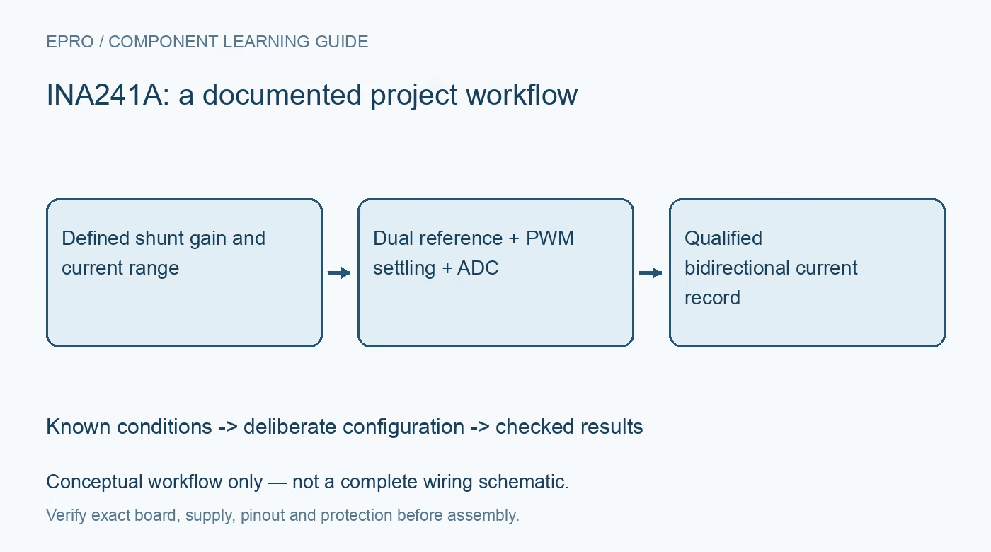
INA241A Current-Sense Amplifier: 7 Checks for Dual References and PWM Sampling
Plan INA241A current sensing with exact gain suffixes, averaged reference inputs, shunt-error budgets and PWM-edge settling checks. This is a documentation-based planning guide, not a report of independent hands-on testing.
1. Identify gain and accuracy grade exactly
INA241A is the higher-accuracy member of a documented A and B family, with fixed-gain suffixes rather than a software gain register. A1 through A5 provide nominal gains of 10, 20, 50, 100 and 200 volts per volt. Read the entire ordering code and use the corresponding electrical table. Do not apply an A-grade offset or gain specification to a B-grade substitute. Preserve package identity as well, since the schematic and board must match the actual pin functions. Manufacturer documentation.
2. Separate amplifier supply from bus common mode
The amplifier supply range is 2.7V to 20V, while the recommended input common-mode range extends from minus 5V to 110V. These are different voltages with different limits. A high common-mode capability does not permit a 110V supply connection or create an isolation barrier. The wider survival range is also not the normal measurement specification. Begin with protected low-voltage sources and assess every input, reference and output pin against its own operating conditions before considering a higher-energy application. Manufacturer documentation.
3. Design around the average of both references
At zero differential input, the output baseline is the average of REF1 and REF2. Connecting both to the same reference places the baseline there; connecting one to supply and the other to ground places it near half supply. Do not assume either reference is an unused optional pin. Choose low-impedance sources and include reference noise and uncertainty in the measurement budget. Verify the actual zero-current baseline with the intended ADC connected rather than subtracting an assumed universal midpoint in software. Manufacturer documentation.
4. Choose the shunt for signal and dissipation
The ideal output change is gain multiplied by current multiplied by shunt resistance, added to the reference baseline. Leave room for positive and negative current within the usable output swing and ADC range. Shunt loss follows current squared multiplied by resistance; lowering resistance reduces heat but makes offset and connection errors more important. Use Kelvin sense routing and account for resistor tolerance and temperature coefficient. A high-accuracy amplifier cannot correct a poorly routed or thermally drifting shunt automatically. Manufacturer documentation.
Newest in the store


5. Make PWM rejection a sampling plan
Enhanced PWM rejection reduces disturbance from changing common-mode voltage, but it does not remove all edge-related error or guarantee instant precision after every transition. Record switching frequency, edge conditions, input network and the chosen sample delay. The documented support for switching frequencies up to 125kHz is conditional, not a universal valid-sample window. Observe the output around both edges in the real low-energy test setup and qualify when samples meet the application error target. Manufacturer documentation.
6. Convert ADC readings with the real baseline
Subtract the established reference-derived baseline before dividing by gain and shunt resistance. Keep units and current polarity explicit, then validate known zero, positive and negative currents using suitable independent equipment. Include output headroom, ADC reference error and any sampling-filter delay. A high-resolution converter does not remove amplifier or shunt uncertainty. Flag saturation, invalid reference conditions and unsettled edge samples instead of presenting every numerical conversion as a valid current measurement. Manufacturer documentation.
7. Preserve the conditions behind current accuracy
Log exact suffix, shunt value and rating, reference connections, supply, common-mode conditions, temperature, PWM timing and raw output or ADC codes. Compare static loading with representative switching operation and repeated zero-current checks. Use current-limited supplies and a reviewed fixture; high bus-voltage ratings are not beginner wiring instructions. Report the measured uncertainty of the assembled path separately from component headlines. This produces a reproducible bidirectional-current record, not a claim that every INA241A board achieves the same system accuracy. Manufacturer documentation.
Related reading: INA240 Current Amplifier: 7 Checks Around PWM Switching.
Catalog note: The exact-part search did not return a matching Epro listing during preparation. Check the current catalog; this guide makes no price, availability or included-accessory claim.