


TMUX1208 Analog Mux: 7 Checks for Active-High Enable and Low-Voltage Paths

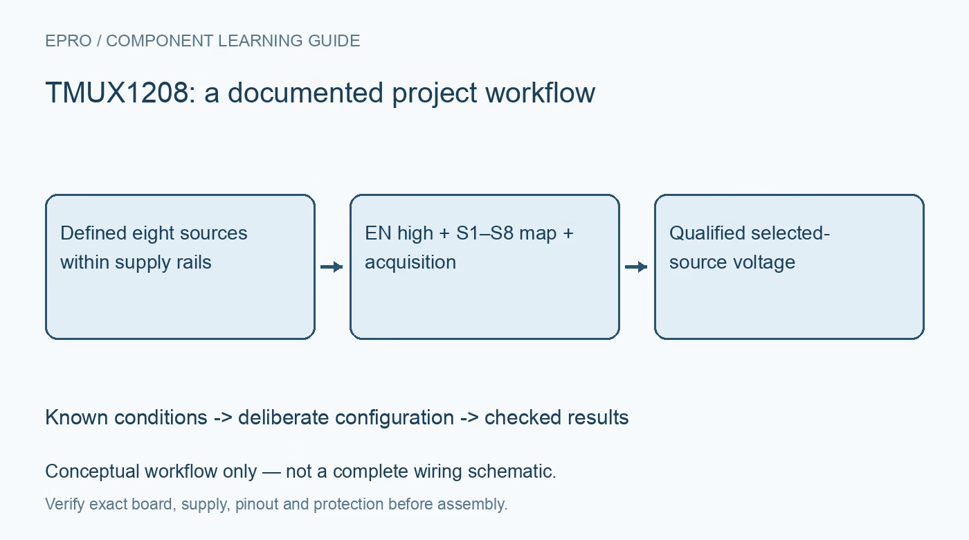
TMUX1208 Analog Mux: 7 Checks for Active-High Enable and Low-Voltage Paths
TMUX1208 checks for active-high enable, S1-to-S8 addressing, low-voltage operation, fail-safe controls and analog settling. This is a documentation-based planning guide, not a report of independent hands-on testing.
1. Verify the exact mux and its signal limits
The TMUX1208 is a single eight-to-one bidirectional analog multiplexer, whereas the TMUX1209 provides a different dual four-to-one arrangement. The recommended supply range is 1.08 V to 5.5 V, with ordinary analog signals constrained between ground and VDD. Low-voltage operation does not provide amplification or isolation. Establish every source range and ground relationship before connecting the mux. A related part with a similar name can have different enable polarity, labeling or protection behavior, so preserve the complete device identity. Manufacturer documentation.
2. Use EN high to connect the selected channel
For this part, EN high enables the addressed path and EN low turns every path off. That polarity differs from some other eight-channel muxes. Define the reset state and address pins deliberately so a startup glitch cannot select an unintended source. Test disabled operation with a known downstream impedance, because an open output can retain charge or float. A plausible ADC code while the mux is disabled is not proof that the selected sensor is connected. Manufacturer documentation.
3. Map binary addresses to S1 through S8
With the mux enabled, A2:A0 equal to 000 selects S1, while 111 selects S8. Channel labels are one-based even when a software array is zero-based. Use eight distinct, bounded source levels to verify the mapping before scanning automatically. Preserve the physical label and software index in the log. A consistent one-position naming error can survive basic communications tests and produce apparently smooth data while associating every measurement with the wrong sensor or connector. Manufacturer documentation.
4. Limit fail-safe reasoning to the control pins
The fail-safe logic feature applies to EN and the address inputs. Those controls can tolerate the documented levels before the supply is present, including the specified 5.5 V control example with VDD at zero. This does not grant unrestricted power-off or overvoltage capability to the analog signal terminals. Check each pin class separately. Likewise, 1.8 V-compatible logic thresholds are a control-interface feature, not permission to pass an analog signal above the operating analog supply rail. Manufacturer documentation.
Newest in the store


5. Include path resistance in the measurement model
The low on-resistance headline is conditional, not an ideal zero-ohm connection across all signals and supplies. Resistance, leakage and source loading can create errors, especially with weak sources or low supply voltage. Evaluate the full path into the destination rather than testing only with a high-impedance meter. Consider signal amplitude, temperature and destination acquisition current. A low nominal resistance does not eliminate the need for a buffer or establish that every sensor can drive a switched-capacitor ADC directly. Manufacturer documentation.
6. Separate break-before-make from completed settling
Break-before-make switching prevents an intentional overlap between selected paths, but charge injection and capacitance can still perturb the output after a channel change. The transition-time specification does not establish final ADC accuracy for an arbitrary source impedance. Analyze the acquisition network and compare readings after alternating large input steps. Choose any delay or discarded conversion from that evidence and the converter timing. Avoid transferring a fixed settling delay from a different mux family or a board with much lower source impedance. Manufacturer documentation.
7. Qualify low-voltage operation with the actual destination
Record VDD, source voltages, address, enable level, destination load, acquisition interval and the final sampled result. Verify every channel, disabled state and controller reset using a protected low-voltage setup. Include the minimum intended supply and the largest normal channel-to-channel step. Keep protection tests distinct from normal accuracy checks and never treat absolute maximum ratings as test targets. The resulting record should establish correct selection and settled data without claiming analog fault protection merely because the logic controls are fail-safe. Manufacturer documentation.
Related reading: TMUX1308 Analog Multiplexer: 7 Checks for Reliable Channel Selection.
Catalog note: The exact-part search did not return a matching Epro listing during preparation. Check the current catalog; this guide makes no price, availability or included-accessory claim.