


TPS22964C Load Switch: 7 Checks for Disabled Reverse Blocking and Discharge

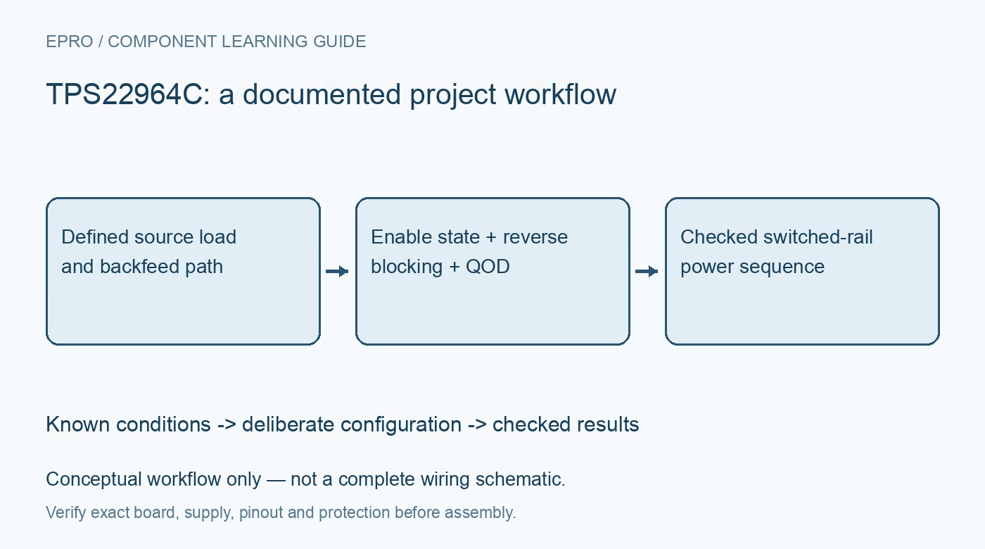
TPS22964C Load Switch: 7 Checks for Disabled Reverse Blocking and Discharge
Plan TPS22964C power gating with state-dependent reverse-current protection, output discharge, fixed startup slew and backfeed checks. This is a documentation-based planning guide, not a report of independent hands-on testing.
1. Identify the discharge-enabled family member
The documented family includes related switches with different output-discharge behavior. TPS22964C provides quick output discharge, while that feature must not be assumed for TPS22963C. Read the complete part and package code before choosing a shutdown strategy. Check the tiny package orientation and board routing carefully, including every supply and ground connection. A current rating or family title does not prove a breakout board has the copper, connector or thermal capability of a reviewed application layout. Manufacturer documentation.
2. Respect the voltage and control conditions
The recommended input range is 1V to 5.5V, with separate output and ON-pin limits. The guaranteed ON thresholds depend on the input-voltage band, so verify the controller high and low levels against the actual operating conditions. Drive a defined off state during controller reset instead of relying on an uncontrolled pin. This is a pass switch, not a regulator. It cannot correct an unsuitable input voltage, and it does not make every connected downstream component tolerant of that rail. Manufacturer documentation.
3. Restrict reverse-blocking claims to disabled operation
The reverse-current protection feature applies when the switch is disabled and the documented voltage conditions are met. The application guidance requires the device to be off and either VIN or VOUT above 1V for the stated behavior. Do not describe it as unconditional bidirectional isolation. When enabled, the path can permit intentional reverse current according to the device architecture. Draw the entire power tree, including USB, debugger and other auxiliary supplies, before deciding whether a disabled switch prevents the backfeed of concern. Manufacturer documentation.
4. Account for discharge when another source is present
When disabled, the discharge-enabled version connects VOUT toward ground through a resistance with a typical value around 273 ohms. This prevents a floating output, but it can also load an external source that intentionally holds VOUT up. Reverse blocking toward VIN and discharge toward ground are separate paths. Estimate that discharge current and resistor dissipation for the actual rail, and verify all applicable limits. Do not assume that a protected upstream input means the downstream alternate supply sees no extra load. Manufacturer documentation.
Newest in the store


5. Budget startup current from the actual load
The device has controlled turn-on behavior, but that does not make it a programmable current-limit controller. Estimate capacitive inrush from output capacitance and rise rate, then include any active downstream load during the ramp. Use the documented waveform conditions and verify the assembled result with a current-limited source. A source collapse can cause repeated startup attempts even if the steady-state load is acceptable. Check both input droop and downstream reset behavior rather than observing only the final output voltage. Manufacturer documentation.
6. Calculate conduction loss with realistic margins
The effective on-resistance headline is about 13 milliohms at specified conditions, distinct from the internal pass-FET figure. Use the appropriate maximum and temperature dependence for design decisions. Conduction loss follows current squared multiplied by resistance; trace and connector losses add to the switch heating. The 3A maximum continuous-current headline is not a guarantee for every tiny module. Start with a modest load and verify the actual board thermal behavior before approaching the intended operating current. Manufacturer documentation.
7. Test each source sequence explicitly
Create a sequence matrix covering input present, input removed, output externally driven, controller reset and normal shutdown within the documented limits. Measure VIN, VOUT, ON, source current and decay time with a protected low-energy setup. Preserve the exact variant, capacitance, discharge behavior and alternate-source arrangement alongside the results. Keep reverse leakage, discharge current and enabled conduction labeled separately. This prevents a useful state-specific protection feature from being presented as a universal backfeed solution. Manufacturer documentation.
Related reading: TPS22992 Load Switch: 7 Checks for Variant Protection and CT Voltage.
Catalog note: The exact-part search did not return a matching Epro listing during preparation. Check the current catalog; this guide makes no price, availability or included-accessory claim.