


TPS22990 Load Switch: 7 Checks for Bias Rails, Power Good and Discharge

TPS22990 Load Switch: 7 Checks for Bias Rails, Power Good and Discharge
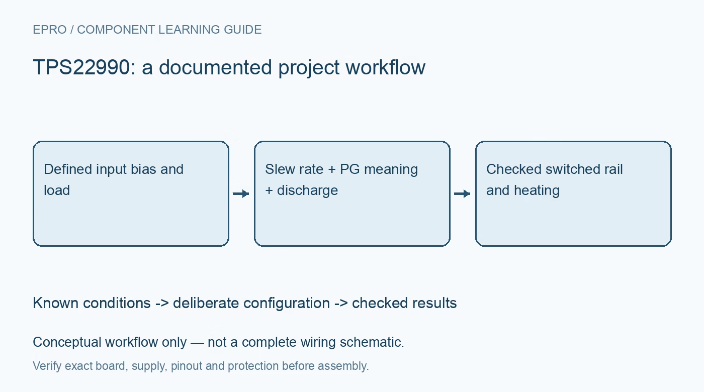
Review TPS22990 bias requirements, controlled inrush, unusual power-good meaning, package grounding and optional output discharge. This is a documentation-based planning guide, not a report of independent hands-on testing.
1. Separate the bias rail from the switched rail
TPS22990 needs a VBIAS supply from 2.5V to 5.5V, while the switched VIN may range from 0.6V up to VBIAS. A low-voltage rail therefore cannot necessarily power the bias input directly. Draw both rails and their sequencing explicitly, including the controller ground reference. Check the actual package orientation and board connections before applying power. This is a controlled pass switch, not a voltage regulator that can correct an unsuitable input or create a higher output. Manufacturer documentation.
2. Inspect the electrically active thermal pad
The exposed thermal pad is associated with VIN, not a generic ground pad. Copying a common thermal-pad-to-ground layout convention can therefore create a direct supply fault. Review the footprint, copper connection and thermal layout against the manufacturer pin-function table. Keep the high-current path appropriately sized and provide local bypassing. Check continuity on an unpowered board before attaching a source. Package power handling depends on the actual board construction, so a small breakout cannot inherit a rating from an unrelated reference layout. Manufacturer documentation.
3. Budget resistance loss and temperature
The headline on-resistance is approximately 3.9 milliohms under specified conditions, and the maximum continuous switch-current rating is 10A. Neither removes thermal or connector constraints. As an illustrative calculation, 8A through 3.9 milliohms dissipates about 0.25W in the pass path before temperature dependence and other losses are considered. Use worst-case specifications and the intended board thermal conditions for design decisions. Include trace, connector and supply limits when selecting a bounded initial load. Manufacturer documentation.
4. Set the ramp from the complete startup load
The CT capacitor adjusts output slew rate. Estimate capacitive inrush using load capacitance multiplied by the output voltage rise rate, then add any load that starts drawing current during the ramp. Choose CT using the documented conditions and verify the resulting waveform because VIN and VBIAS affect timing. A slower ramp can reduce source droop but also prolong operation in an intermediate-voltage region. Do not treat controlled slew rate as an independent short-circuit current limiter or electronic fuse. Manufacturer documentation.
Newest in the store


5. Read PG as switch readiness, not regulation
The PG output indicates that the pass-FET gate has been driven high and the switch on-resistance is close to its final value. It is not a precision comparator proving that VOUT reached a specified percentage of VIN. PG is active high and open drain, so provide a suitable pullup; VBIAS must be present for a valid output. If the application requires a precise downstream voltage threshold, qualify it with an appropriate monitor rather than inferring it from this flag. Manufacturer documentation.
6. Account for the discharge variant
TPS22990 includes a typical 218-ohm output-discharge path when disabled; TPS22990N omits this feature. Determine which version is fitted before predicting rail decay. Output discharge can interact with a prebiased load or another supply feeding the same rail, so check the entire power tree and avoid unintended current paths. ON is active high and must not float. Test disabled-state decay with the actual output capacitance and load instead of assuming that every board shuts down at the same speed. Manufacturer documentation.
7. Exercise sequencing with a protected source
Use a current-limited supply and modest load to inspect VBIAS, VIN, ON, VOUT and PG during startup and shutdown. Repeat the allowed sequencing cases and observe rail droop, rise time and temperature before increasing current. Do not assume reverse-current blocking or fault isolation unless the documented conditions explicitly provide it. Save the fitted variant, capacitor values, source limits and waveforms with the project. These observations establish evidence for one implementation, not a universal validation of every module sold under the part name. Manufacturer documentation.
Related reading: TPS22975 Load Switch: 7 Checks for Bias Supply and CT Capacitor Ratings.
Catalog note: The exact-part search did not return a matching Epro listing during preparation. Check the current catalog; this guide makes no price, availability or included-accessory claim.