


UCC27517 Gate Driver: 7 Checks for Input Interlocks and Gate Loading

UCC27517 Gate Driver: 7 Checks for Input Interlocks and Gate Loading
UCC27517 checks for dual-input interlocks, a single gate output, supply limits, peak-current meaning and low-voltage validation. This is a documentation-based planning guide, not a report of independent hands-on testing.
1. Confirm the low-side single-output architecture
The UCC27517 is a single-channel low-side gate driver with one OUT terminal. Unlike split-output drivers, it does not expose separate sourcing and sinking pins for independent gate-resistor paths. It is not galvanically isolated and does not provide a high-side bootstrap supply. Confirm the exact package pinout and local ground reference before planning connections. For initial work, leave any transistor power stage disconnected and use only a benign capacitive gate-equivalent load supplied from a protected, current-limited low-voltage fixture. Manufacturer documentation.
2. Apply the dual-input condition explicitly
OUT is driven high only when IN+ is high and IN− is low. A low IN+ or a high IN− therefore disables the high output state. This makes the second input useful for an interlock, but it is not a separate isolated safety channel. For noninverting drive, define IN− low and drive IN+; for inverting drive, define IN+ high and drive IN−. Write this truth table into the control specification and test all combinations before connecting a switched load. Manufacturer documentation.
3. Define floating and reset states deliberately
Internal biasing is arranged to hold the output low when inputs float. However, normal enabled operation requires the unused input to be correctly biased; leaving it floating is not the way to obtain a reliable enabled driver. Include controller reset, connector removal and supply-ramp conditions in the design review. Verify the actual voltage at both input pins. A firmware interlock variable says nothing about the physical state before the controller has configured its GPIO direction and output level. Manufacturer documentation.
4. Review supply and UVLO with gate-voltage limits
The recommended supply range is 4.5 V to 18 V. Undervoltage lockout holds OUT low below its operating threshold, but a typical UVLO transition is not a substitute for the recommended supply limits. Output drive follows the driver supply, so a compatible driver voltage must also respect the transistor gate-source rating and ringing margin. Use appropriate local decoupling. Do not attach a grounded oscilloscope clip to an unknown switching reference or energized high-voltage circuit while checking these signals. Manufacturer documentation.
Newest in the store


5. Distinguish peak gate current from load current
The advertised 4 A source and 4 A sink capabilities are peak gate-drive figures under stated conditions, including the specified driver supply. They are not continuous output-current ratings and do not describe the motor, converter or other power-stage load current. Estimate average gate-drive demand from gate charge, voltage and frequency, then consider internal and resistor dissipation. A larger capacitor or a faster switching rate can raise heating substantially even when the output voltage and truth table initially look correct. Manufacturer documentation.
6. Preserve timing margin through the physical layout
The input thresholds are designed for compatible low-voltage logic independently of the driver supply, but thresholds, hysteresis and noise margin still require checking. Typical propagation and edge times depend on the test load and supply. Keep the output-current loop, bypass capacitor and ground return compact, and avoid long shared return paths that inject gate current into input references. Evaluate any filter or gate resistor as part of the complete timing path rather than assuming every extra RC network improves reliability. Manufacturer documentation.
7. Qualify the interlock before reviewing a power stage
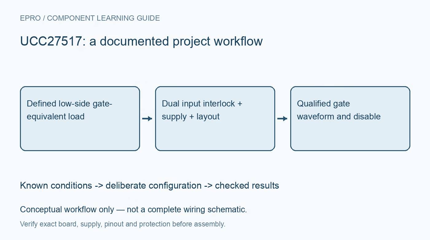
With the gate-equivalent load only, record supply, both input states, output amplitude, disable response, edge shape and temperature. Exercise each interlock transition and the complete power-up and power-down cycle. This validates only the bounded driver fixture, not switching losses, transistor protection or high-voltage safety. A power-stage connection needs a separate topology and protection review with suitable instrumentation. Preserve that boundary in the test report so a successful low-side gate waveform is not presented as a complete safe converter design. Manufacturer documentation.
Related reading: UCC27511 Gate Driver: 7 Checks Before Connecting a Power Stage.
Catalog note: The exact-part search did not return a matching Epro listing during preparation. Check the current catalog; this guide makes no price, availability or included-accessory claim.