


UCC27511 Gate Driver: 7 Checks Before Connecting a Power Stage

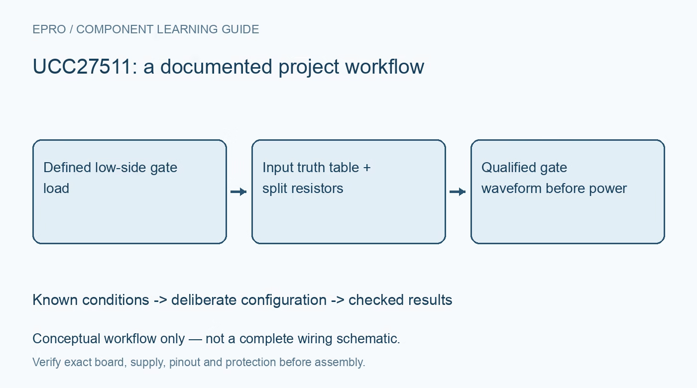
UCC27511 Gate Driver: 7 Checks Before Connecting a Power Stage
UCC27511 checks for low-side topology, split gate outputs, input truth tables, UVLO and safe low-voltage verification. This is a documentation-based planning guide, not a report of independent hands-on testing.
1. Identify what the driver can and cannot drive
The UCC27511 is a single-channel low-side gate driver, not an isolated driver and not a bootstrap high-side supply. Its reference is local ground, and its output swing follows the driver supply. Select the topology before considering peak-current headlines. A suitable transistor still needs an independently reviewed power circuit, protection and layout. For initial verification, leave the power stage disconnected and use a benign capacitive gate-equivalent load on a current-limited low-voltage bench supply. Manufacturer documentation.
2. Match supply voltage to the transistor gate limits
The recommended driver supply range is 4.5 V to 18 V. That range does not mean every MOSFET gate can tolerate the upper end, including ringing. Check the transistor gate-source rating, desired on-state drive and the driver operating limits together. Place appropriate local bypassing near the driver and keep return paths short. Plan measurements around the actual reference potential; never connect a grounded instrument clip to an unknown switching node or energized high-voltage circuit. Manufacturer documentation.
3. Use the two-input truth table deliberately
The output is high only when IN+ is high and IN− is low. For noninverting operation, drive IN+ and define IN− low; for inverting operation, drive IN− and define IN+ high. Do not confuse the minus input with an analog differential-amplifier terminal. Verify all four input combinations with the dummy load and include controller startup states. Internal input biasing supports disabled behavior, but external control signals should still have deliberate, documented idle levels. Manufacturer documentation.
4. Understand why OUTH and OUTL are separate
The UCC27511 exposes separate sourcing and sinking output paths so that turn-on and turn-off gate resistances can be selected independently. These are not two independently commanded load outputs. Follow the exact device pinout and recommended connection arrangement; a related family member may expose a different output structure. Choose resistor values from gate charge, desired switching behavior, ringing and dissipation. Begin conservatively and change one parameter at a time rather than shorting the paths into an unreviewed layout. Manufacturer documentation.
Newest in the store


5. Do not convert peak current into a continuous rating
The 4 A source and 8 A sink figures describe peak gate-drive capability, not allowable continuous output current or the switched load current. Average gate-drive demand depends on gate charge, switching frequency and drive voltage. A useful first-order power estimate is gate charge multiplied by drive voltage and frequency, with additional losses considered separately. Evaluate package temperature and bypass-current loops under the actual waveform. A large peak-current specification cannot compensate for inadequate copper or long inductive connections. Manufacturer documentation.
6. Check UVLO and timing under stated conditions
Undervoltage lockout holds the outputs low when the supply is insufficient; it is not a substitute for operating within the recommended supply range. The typical turn-on threshold is about 4.2 V with approximately 300 mV hysteresis, but use the specified limits when planning sequencing. Published propagation and rise/fall figures depend on test conditions. Slow or noisy input transitions and ground bounce can produce unwanted behavior, so avoid assuming an arbitrary input RC filter is harmless. Manufacturer documentation.
7. Record a disconnected-power-stage acceptance test
With only the benign capacitive load connected, document input polarity, disabled states, supply ramp behavior, output amplitude, edge shape and temperature. Check both turn-on and turn-off paths before changing resistor values. A successful dummy-load test qualifies only that fixture; it does not validate transistor switching losses, isolation or high-voltage safety. Connecting the power stage requires a separate design review and suitable protected instrumentation. Keep this distinction explicit so that a convincing gate waveform is not mistaken for a complete safe converter. Manufacturer documentation.
Related reading: IRF520 Arduino Modules: Check the Actual Gate-Driver Circuit.
Catalog note: The exact-part search did not return a matching Epro listing during preparation. Check the current catalog; this guide makes no price, availability or included-accessory claim.