


Bi Directional Logic Level Converter: 7 Buying Checks

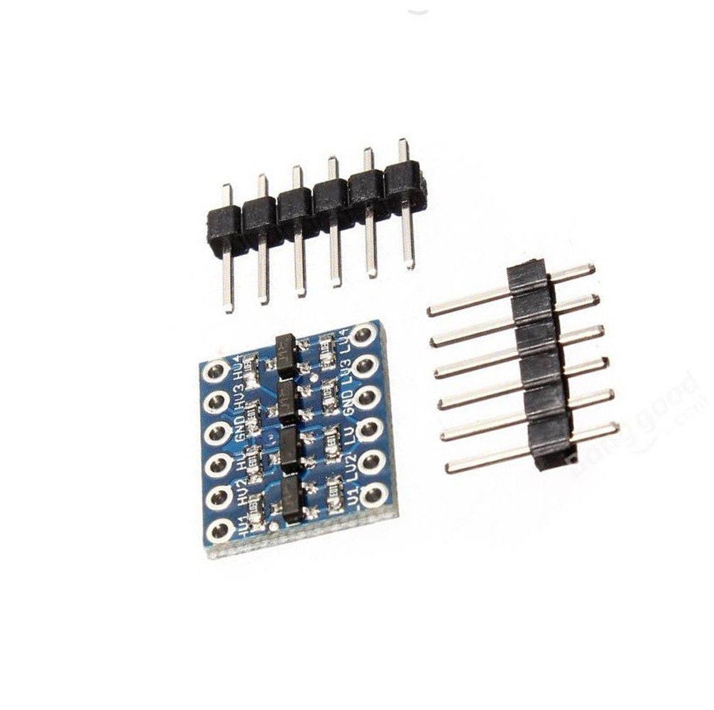
A bi directional logic level converter helps compatible digital devices communicate across different logic-voltage domains. A common example is a 3.3 V controller talking to a 5 V I2C peripheral without exposing its GPIO to the higher bus voltage.
The word converter can be misleading. This small signal board is not a DC power regulator, an analog scaling circuit, a motor driver or electrical isolation. Choosing the right circuit starts with the signals and their timing.

Bi directional logic level converter prices and board types
| Listed item | Price (PKR) | Project role |
|---|---|---|
| 4-Channel 3.3V / 5V Bi-Directional Logic Level Converter Module in Pakistan | 100 | Four-channel converter requiring both voltage references |
| 5V to 3V Logic Level Converter – 4 Channel Module Adapter in Pakistan | 115 | Different four-channel board listing describing an onboard regulator |
Price snapshot: Epro listings checked on 18 October 2026. Confirm the current price, availability, delivery charges and package quantity on the linked page before ordering. These are dated listing prices, not a quotation or an independent performance test.
The four-channel bidirectional module requires the high and low voltage references used by the system. The alternative converter listing describes extra power circuitry. Do not assume the boards have identical power wiring because both advertise four channels.
1. Identify the circuit and pin labels
The common MOSFET-and-pull-up design provides paired high-side and low-side signal connections. Labels such as HV1 and LV1 identify the same channel on different voltage domains. HV and LV without a number are reference supplies, not a fifth signal channel.
The SparkFun converter guide explains this general arrangement. Its diagram is a circuit reference, not proof that every unbranded board uses identical components or includes the same additional circuitry.
2. Separate signal translation from power conversion
A basic converter needs a regulated low reference and a regulated high reference already available. Connecting 5 V to HV does not automatically produce a usable 3.3 V supply at LV. That pin normally receives the low reference rather than creating it.
If a particular board adds a regulator, follow that exact board’s documented power connections and current limits. Never infer regulator capability from a familiar blue PCB or a product name. A signal channel must not be used to power a sensor, display or motor.
3. Choose an appropriate signal type
The standard pull-up MOSFET arrangement is especially useful for open-drain buses such as I2C. It allows a low asserted on either side to be recognised on the other while each side rises to its own reference through pull-ups.
Newest in the store


Other protocols need a closer look at direction, output type and timing. Do not promise that one inexpensive four-channel board handles every fast push-pull interface. Never connect two actively opposing outputs to the same channel and expect the converter to resolve the conflict safely.
4. Review pull-ups and rise time
Pull-up resistance and bus capacitance affect how quickly the signal returns high. Long leads, multiple boards and several parallel pull-ups can change behaviour. A device answering once at low speed is not proof that a long bus will work reliably at a faster setting.
For a first I2C test, keep wiring short and begin with a modest bus speed compatible with all devices. Validate the actual arrangement before increasing speed. A logic analyser or oscilloscope can help investigate timing, but it does not replace a correct voltage-domain design.
5. Use both references and common ground
In a 3.3 V-to-5 V system, LV connects to the regulated 3.3 V reference and HV to the regulated 5 V reference. The communicating devices and converter share the intended ground. Channel one must connect through its matching LV1 and HV1 pair.
This common-ground design is not galvanic isolation. It is unsuitable as a casual way to join hazardous voltages, mains-referenced circuits or unknown ground potentials. Those applications require an appropriately engineered isolated interface.
6. Keep analog and power signals out
A varying analog sensor voltage is not translated proportionally by this digital converter. Use an appropriate analog conditioning design for an ADC input. Likewise, USB, HDMI and other specialised high-speed links need interfaces designed for their electrical requirements.
Do not apply 12 V or 24 V merely because those terms appear in online search suggestions. The particular board and connected GPIO must remain within their documented limits. This guide addresses the listed 3.3 V/5 V digital arrangement only.
7. Test a simple bus before a full project
Follow the logic level converter wiring guide for a classic ESP32 and a compatible 5 V I2C peripheral. Verify rails and channel pairs before powering the circuit. An I2C acknowledgment is a useful connection check, not proof that every peripheral function or operating condition has been validated.