


DAC8552 Dual DAC: 7 Checks for Buffers and Shared Updates

DAC8552 Dual DAC: 7 Checks for Buffers and Shared Updates
Plan DAC8552 outputs with seven checks for external reference, 24-bit frames, buffer selection, shared updates, zero-scale reset and power-down. This is a documentation-based planning guide, not a report of independent hands-on testing.
1. Confirm the reference and pin functions before reuse
DAC8552 is a dual sixteen-bit voltage-output DAC operating from 2.7 V to 5.5 V. Its VREF pin is an external reference input; there is no internal-reference enable command to borrow from DAC8562. The eight-pin interface also has no physical LDAC input. Verify supply, ground, both outputs, reference and serial pins against the exact package drawing. A similar product name or pin count is not sufficient evidence that a previously used DAC library has the right command format. Manufacturer documentation.
2. Calculate ideal codes without promising rail performance
The nominal transfer equation is VOUT = VREF multiplied by code divided by 65536. With a 2.5-V reference, code 32768 ideally requests 1.25 V, and code 65535 remains one ideal step below the reference. Offset, gain error, reference error, output loading and available headroom determine the real result. Use a stable reference within the specified range, bypass it as recommended, and measure it at the device. Supply noise is not removed simply because the command has sixteen data bits. Manufacturer documentation.
3. Build an explicit twenty-four-bit serial transaction
Each transfer contains eight control bits followed by sixteen data bits, shifted most-significant bit first on falling SCLK edges while SYNC is low. The two highest control bits must be zero. The selected action is decoded on the twenty-fourth falling clock edge; it does not wait for SYNC to rise. Raising SYNC earlier aborts an incomplete command. Verify actual edges and bit order with a logic analyzer, and meet the specified delay before starting the next transfer. Manufacturer documentation.
4. Keep buffer selection distinct from output loading
The Buffer Select bit chooses whether the incoming data or power-down command enters buffer A or B. Separate LDA and LDB bits control which DAC output registers are updated. Those roles are not interchangeable, and the control matrix permits writing one buffer while loading another output. Represent the fields explicitly in firmware and test them with different safe output codes. A successful serial transmission can still leave the intended analog output unchanged if the command only stored a buffer value. Manufacturer documentation.
Newest in the store


5. Plan a coordinated two-channel update without LDAC
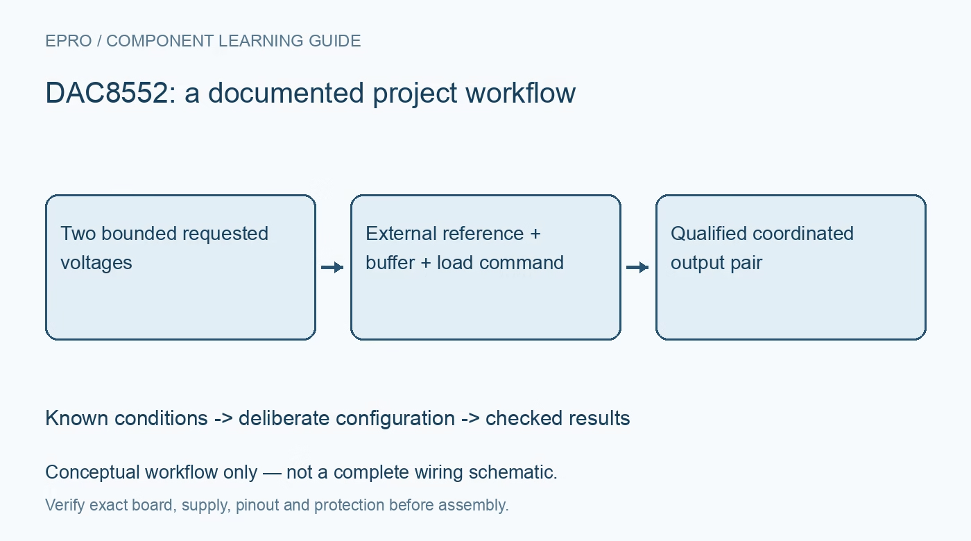
To stage two new values, first write buffer A without loading an output. A subsequent command can write buffer B and request loading both DACs, transferring the prepared pair into the output registers together. Validate the exact control matrix rather than assuming a generic broadcast command. Simultaneous register loading does not mean the two analog outputs settle with zero skew or equal load response. Observe both outputs and quantify settling before using the pair as a coordinated stimulus. Manufacturer documentation.
6. Distinguish zero-scale reset from power-down impedance
Power-on reset sets DAC output registers to zero-scale until valid write-and-load operations occur. That is not the same state as selecting a high-impedance power-down output. The power-down commands offer typical 1-kilohm, 100-kilohm or high-impedance output configurations, applied through the buffer/load controls. Recovery requires a normal-operation command and the appropriate load action. Do not drive digital pins high before the device is powered; review upstream host sequencing and downstream circuitry that could feed an unpowered output. Manufacturer documentation.
7. Validate each command against a measured output pair
Start with unloaded outputs connected only to suitable high-impedance measurement equipment. Check low, middle and high codes within a deliberately bounded range, then test buffer-only writes, single-channel loads, shared loads and power-down recovery. Record reference voltage, supply, command bytes, both measured outputs and settling time. Only add the real load after checking its capacitance and current demand. This creates a reproducible command-to-voltage record without confusing an ideal code calculation or manufacturer plot with an independently tested result. Manufacturer documentation.
Related reading: DAC8562 Dual DAC: 7 Checks for Reference, Gain and LDAC.
Catalog note: The exact-part search did not return a matching Epro listing during preparation. Check the current catalog; this guide makes no price, availability or included-accessory claim.