


TLC59282 LED Driver: 7 Checks for Transparent Latches and Blanking

TLC59282 LED Driver: 7 Checks for Transparent Latches and Blanking
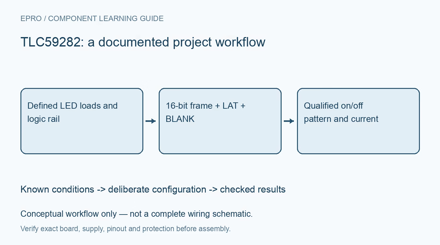
TLC59282 checks for its 16-bit on/off register, transparent LAT behavior, blanked startup, current setting and grouped delays. This is a documentation-based planning guide, not a report of independent hands-on testing.
1. Start with on/off control rather than grayscale assumptions
The TLC59282 controls sixteen constant-current sink outputs with one on/off bit per channel. It does not contain the twelve-bit grayscale engine found in some other LED drivers. Establish whether the application needs binary indicators, externally managed brightness or another architecture before selecting it. The logic supply range is 3 V to 5.5 V, while output terminals have a separate 17 V capability. Neither the LED-voltage rating nor a similar package makes the logic pins high-voltage tolerant. Manufacturer documentation.
2. Match controller levels to the actual supply
The high-input requirement is 0.7 times VCC, so a driver powered at 5 V requires a guaranteed input high of at least 3.5 V. A 3.3 V microcontroller output is therefore not automatically compliant. Select compatible rails or a suitable translator and include BLANK and LAT in the level review, not just serial data and clock. Check the waveform at the driver input under the real wiring load rather than inferring margin from the controller supply label. Manufacturer documentation.
3. Keep outputs blanked until known data is stored
The sixteen-bit shift register and output latch do not power up with a guaranteed default pattern. BLANK high forces all outputs off and should be maintained while a known pattern is written. Set bits for unconnected outputs to zero as the documentation recommends. Only enable the intended channels after supply and control states are established. Internal weak biasing is useful context, but a reviewed reset circuit must account for controller pins, cables and power sequencing rather than relying on a software initialization routine alone. Manufacturer documentation.
4. Treat LAT as a transparent level control
LAT is not merely an edge-triggered snapshot input. While LAT is high, changes in the shift register continue to transfer into the output latch; LAT low holds the stored data. Keep LAT low while shifting an ordinary complete sixteen-bit pattern, then transfer and return it low before further shifting. If clocks occur while LAT remains high, intermediate patterns can reach the outputs. A protocol copied from an edge-latched driver can therefore produce unexpected visible changes even when the frame length is correct. Manufacturer documentation.
Newest in the store


5. Verify serial and cascade timing independently
SIN enters the shift register on rising SCLK edges, moving data toward its most-significant stage. SOUT also changes on rising SCLK edges, so cascade timing must follow this part’s setup, hold and propagation requirements rather than an assumed falling-edge convention. Use a single-channel walking-bit test to establish output order before attaching many LEDs. The 35 MHz headline is conditional on specified timing and loading. A reliable short bench connection does not prove that the same clock works through every longer chain. Manufacturer documentation.
6. Calculate current and dissipation together
One IREF resistor programs the full-on current of all channels. The typical equation gives RIREF in kilohms as 1.205 V multiplied by 41.9 and divided by output current in milliamperes; 10 mA corresponds to approximately 5.05 kilohms. Use the current range appropriate to the operating supply and allow for tolerances. The higher current capability depends on VCC. Check output compliance, simultaneous-channel dissipation and board temperature instead of treating one channel’s current headline as the thermal capacity of the entire package. Manufacturer documentation.
7. Account for grouped switching rather than simultaneous edges
The outputs switch in four documented groups with approximately 20 ns typical spacing to reduce surge noise. Those groups are not simply four adjacent pin ranges, and both turn-on and turn-off are delayed. Preserve the manufacturer grouping when precise edge relationships matter. Test blanking, latch updates, current and supply disturbance using a modest load and current-limited supply. The acceptance record should distinguish channel state, intentional group delay and unintended intermediate patterns; this guide does not establish high-power lighting or optical safety compliance. Manufacturer documentation.
Related reading: TLC5947 LED Driver: 7 Checks for Safe Startup and PWM Frames.
Catalog note: The exact-part search did not return a matching Epro listing during preparation. Check the current catalog; this guide makes no price, availability or included-accessory claim.