


ADS1220 Arduino: 7 SPI and Fresh-Conversion Checks

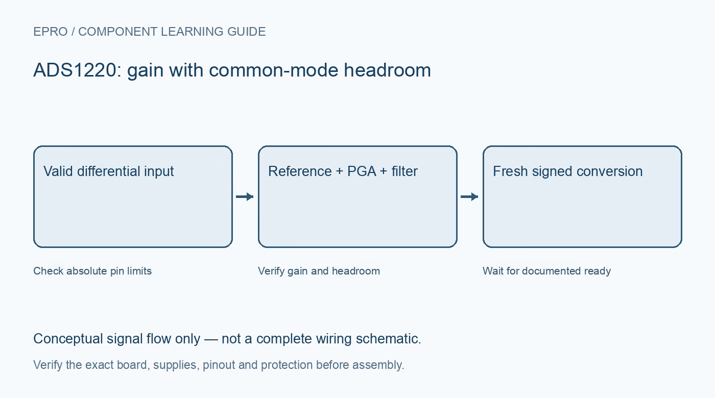
An ADS1220 Arduino integration should prove communication and conversion freshness before attempting a precision sensor project. This workflow uses a documentation-checked low-voltage source and a driver matched to the exact converter. It is not a complete schematic or a claim that example readings have been calibrated.
Verify power before attaching the host
Inspect the carrier for supply and reference routing. Match host outputs and converter digital levels rather than assuming every Arduino is a five-volt Uno or every breakout accepts five-volt logic. Connect the intended grounds and keep the analog source within both input and common-mode limits.
Set the correct SPI clock phase
The ADS1220 supports mode one, with clock idle low and the required phase relationship. Configure that explicitly in the driver and check chip-select framing. Start with a conservative documented clock rate. A response observed with another mode is not sufficient evidence that register traffic is reliable.
Read back a known configuration
Start from documented reset behavior and write an explicit channel, gain, reference, mode and rate. Read the configuration registers back and compare the intended bits. Keep the configuration with each experiment so that a later gain change cannot silently reuse an obsolete voltage conversion factor.
Use a valid first input arrangement
For a ground-referenced test, choose a supported PGA-bypass configuration when appropriate and verify the resulting restrictions. Do not retain a high-gain enabled PGA setting that requires input common-mode headroom above ground. Begin with a known small positive differential voltage rather than an unknown sensor output.
Wait using a working ready signal
Trigger the documented start or synchronization sequence and wait for completion. Dedicated DRDY and shared DOUT/DRDY are not interchangeable in every chip-select state: a three-stated shared output cannot report readiness while deselected. Follow the driver design instead of treating any sampled high level as a new conversion.
Decode signed data with reference and gain
Read the documented twenty-four-bit result completely and sign-extend it correctly before scaling. Use the configured reference and gain, preserving negative differential values where valid. Check the driver return type so sign extension or conversion to volts is not applied twice to an already processed reading.
Newest in the store


Separate failure from a valid zero
Use timeouts and explicit unavailable states for transfer or ready failures. After changing channels or settings, follow the documented restart and settling procedure before assigning the new channel label. Test safe software misconfiguration and recovery, and retain sample age rather than repeatedly presenting a cached number as current.
Frequently asked questions
Why does a ground-referenced input misbehave at high gain?
The enabled PGA can be outside its valid common-mode range even when the differential voltage looks small.
Can a ready timeout mean zero volts?
No. A timeout describes missing evidence, not a measured zero.
Availability and illustration note
No matching Epro product was returned by the catalog search on 21 October 2026 UTC. This learning guide does not assert stock, a selling price or compatibility of an unidentified substitute. The illustration is an original conceptual signal-flow diagram, not a product photograph or complete wiring schematic.
Related Epro reading
For a first bench setup, review breadboard connections and continuity checks and I2C voltage-level translation. These guides do not replace the exact module schematic.
Technical references and limitations
Source: Texas Instruments ADS1220 datasheet. Electrical limits apply to the named part, not automatically to every carrier board. This is a documentation-based learning workflow, not a claim of independent hardware testing, traceable calibration or safety certification.