


ADS7054 SAR ADC: 7 Checks for Differential Sampling and Calibration

ADS7054 SAR ADC: 7 Checks for Differential Sampling and Calibration
Use ADS7054 with correct differential common mode, AVDD reference drive, previous-sample serial timing and explicit offset-calibration frames. This is a documentation-based planning guide, not a report of independent hands-on testing.
1. Separate differential range from terminal voltage limits
ADS7054 is a fourteen-bit, one-megasample-per-second differential SAR converter. Its differential full-scale range extends from negative AVDD to positive AVDD, but that does not allow either input pin to swing arbitrarily below ground. Each input has supply-related limits, and the required common mode is near AVDD divided by two within the documented tolerance. Check both input voltages as well as their difference. A bipolar differential measurement can be implemented with unipolar individual terminals; confusing those two descriptions can overstress the input network. Manufacturer documentation.
2. Treat AVDD as the conversion reference
The converter uses its analog supply as the voltage reference, so reference quality and analog supply behavior directly affect scaling. Provide the documented local bypassing and a source able to support the conversion charge demand. Do not assume a noisy general-purpose rail becomes a precision reference merely because the digital interface works. AVDD and DVDD have their own operating limits and can be independent, but the complete power sequence and logic levels still require review. Record the actual analog reference condition with calibration data. Manufacturer documentation.
3. Budget acquisition before the sampling edge
The falling edge of CS captures the input and begins conversion. Before that edge, the sampling network must have enough time to acquire the differential signal from the real source impedance. Include amplifier settling, protection resistance, filter capacitance and switched-capacitor loading. The documented minimum acquisition interval is not proof that every external source settles adequately in that time. Test a demanding safe input change and establish the accepted timing from the required accuracy rather than from a convenient serial transfer rate alone. Manufacturer documentation.
4. Distinguish conversion clocks from the bits being read
A normal conversion requires at least eighteen SCLK falling edges within its frame. The data shifted out during that frame represent the previous conversion, not the sample just captured. The output includes a leading zero and the fourteen conversion bits in the documented timing arrangement. Too few clocks invalidate the following conversion result. Model the one-frame pipeline explicitly, discard startup or otherwise invalid values and keep sample identity separate from SPI completion time. Reading fourteen bits alone is not sufficient to complete the conversion process. Manufacturer documentation.
Newest in the store


5. Use the correct startup and runtime calibration frames
Offset calibration uses a twenty-four-clock first frame at power-up, whereas the documented recalibration procedure during normal operation uses sixty-four clocks. Do not interchange those procedures or assume an incomplete extended frame completes calibration. Calibration output and startup zeros are not measurements of a zero-volt input. Allow the required acquisition interval afterward and mark the interruption in the record. Recalibration is recommended after significant operating-condition changes, but it corrects internal offset rather than every reference, source or external analog-chain error. Manufacturer documentation.
6. Decode signed codes against the transfer table
The output transfer table gives zero input near code 0000h, positive full scale near 1FFFh and negative full scale near 2000h. Implement the signed fourteen-bit interpretation rather than treating the raw word as an unsigned voltage count. Account for the leading bit placement and host word alignment separately. Verify polarity using safe known differential inputs before applying calibration. Keep raw codes available during development so a sign-extension or pipeline error cannot be disguised by plausible-looking scaled values. Manufacturer documentation.
7. Qualify complete samples under stated conditions
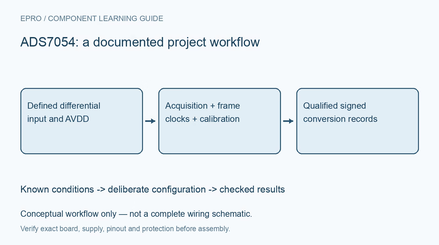
Check input common mode, reference stability, clock count and acquisition timing together, then exercise startup and a deliberate runtime calibration. Confirm which records are invalid or unavailable during those events. Evaluate analog accuracy with an appropriate reference and stated bandwidth, not only a self-consistent serial parser. This article supplies no independent ADC noise or accuracy measurements. Preserve the source network, AVDD condition and calibration epoch so later firmware or filter changes can be assessed against a reproducible conversion workflow. Manufacturer documentation.
Related reading: ADS7056 SAR ADC: 7 Checks for 14-Bit Frames and Previous-Sample Identity.
Catalog note: The exact-part search did not return a matching Epro listing during preparation. Check the current catalog; this guide makes no price, availability or included-accessory claim.