


ADS8320 SAR ADC: 7 Checks for Input Limits and Clock Frames

ADS8320 SAR ADC: 7 Checks for Input Limits and Clock Frames
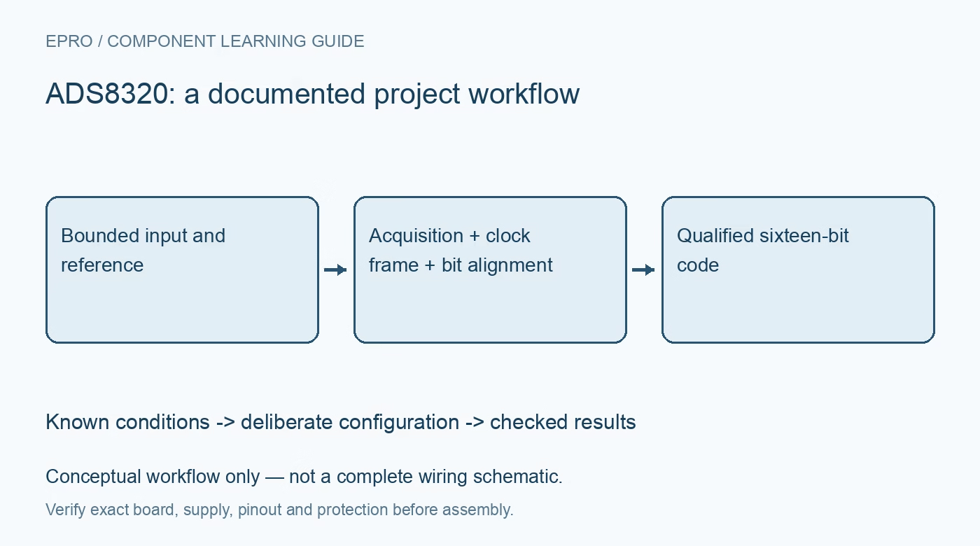
Review ADS8320 input limits, reference drive, acquisition time and serial framing without assuming a sixteen-clock transaction or previous-sample pipeline. This is a documentation-based planning guide, not a report of independent hands-on testing.
1. Distinguish differential sampling from unrestricted common mode
ADS8320 samples the difference between its two inputs, but the negative input has a restricted voltage range near ground. The datasheet gives a narrower negative-input range at a 2.7 V supply than at higher supply conditions. This is not a fully differential converter accepting an arbitrary midrail signal pair. Check the positive and negative pin limits separately, and then check the differential span. Use the negative input as the documented local or remote ground sense where appropriate. Manufacturer documentation.
2. Provide the external reference as a dynamic analog source
The external reference determines the conversion span and must stay within its documented range relative to VCC. It also supplies dynamic current during conversion, so a precise DC voltage reading alone does not prove adequate reference drive. Follow the reference bypassing and layout guidance, including the effects of any buffer and capacitor network. Lowering the reference reduces code size, but can make existing offset and noise larger in code units. It does not automatically improve absolute accuracy. Manufacturer documentation.
3. Allow the input to settle during acquisition
The internal capacitor array must charge from the source during the acquisition interval, specified in clock cycles. High source resistance or an oversized filter can prevent sixteen-bit settling even for a slowly changing signal. Evaluate the driver, filter resistance, capacitance and clock rate as a network. A high static input impedance during hold does not eliminate the charging demand during acquisition. Verify the source can recover after each sample before claiming performance at the maximum conversion rate. Manufacturer documentation.
4. Clock the complete conversion rather than only sixteen bits
The basic timing diagram requires at least twenty-two clock cycles for a sixteen-bit conversion and illustrates a twenty-four-clock transaction. Acquisition, the initial output indication and data alignment must all be handled. Do not implement a generic sixteen-clock transfer solely because the numerical result is sixteen bits wide. Match chip-select setup, clock high and low times and the sampling edge to the datasheet. Use a captured transaction to locate the MSB and LSB unambiguously. Manufacturer documentation.
Newest in the store


5. Keep current-conversion data distinct from pipeline behavior
ADS8320 provides data for the conversion currently in progress; the manufacturer states that there is no pipeline delay. That differs from ADCs that output a previous conversion while starting a new one. If CS stays low and clocks continue after completion, an additional LSB-first data stream can appear. Extra clocks are therefore not evidence of a second independent sample. End and restart transactions deliberately so software sample indexing matches actual acquisition events rather than whichever word length the host interface happens to prefer. Manufacturer documentation.
6. Respect clock limits while reducing average power
The internal sampling architecture imposes both minimum and maximum clock requirements; slowing the serial clock arbitrarily is not a universal low-power strategy. The datasheet describes reduced average power by converting promptly and spending time powered down between samples. CS high also places the device in its documented power-down condition. Include reference, buffer and host consumption in the full system budget. A low sample rate and a slow conversion clock do not necessarily produce the same analog behavior or energy use. Manufacturer documentation.
7. Validate decoding with known inputs and repeatable timing
Apply several safe input voltages across the approved range, including near zero and near the selected reference without exceeding pin limits. Compare raw frames, decoded codes and the predicted reference-based scale. Repeat after changing clock rate and source impedance to expose acquisition errors. Log reference voltage, supply, frame length and sample interval. Separate transfer failures from genuine zero or full-scale values. This documentation-based guide does not claim measured linearity or noise performance for an untested assembly. Manufacturer documentation.
Related reading: ADS7052 SAR ADC: 7 Checks for Previous-Sample Data and Calibration.
Catalog note: The exact-part search did not return a matching Epro listing during preparation. Check the current catalog; this guide makes no price, availability or included-accessory claim.