


ADS8325 SAR ADC: 7 Checks for Input Limits and Complete Frames

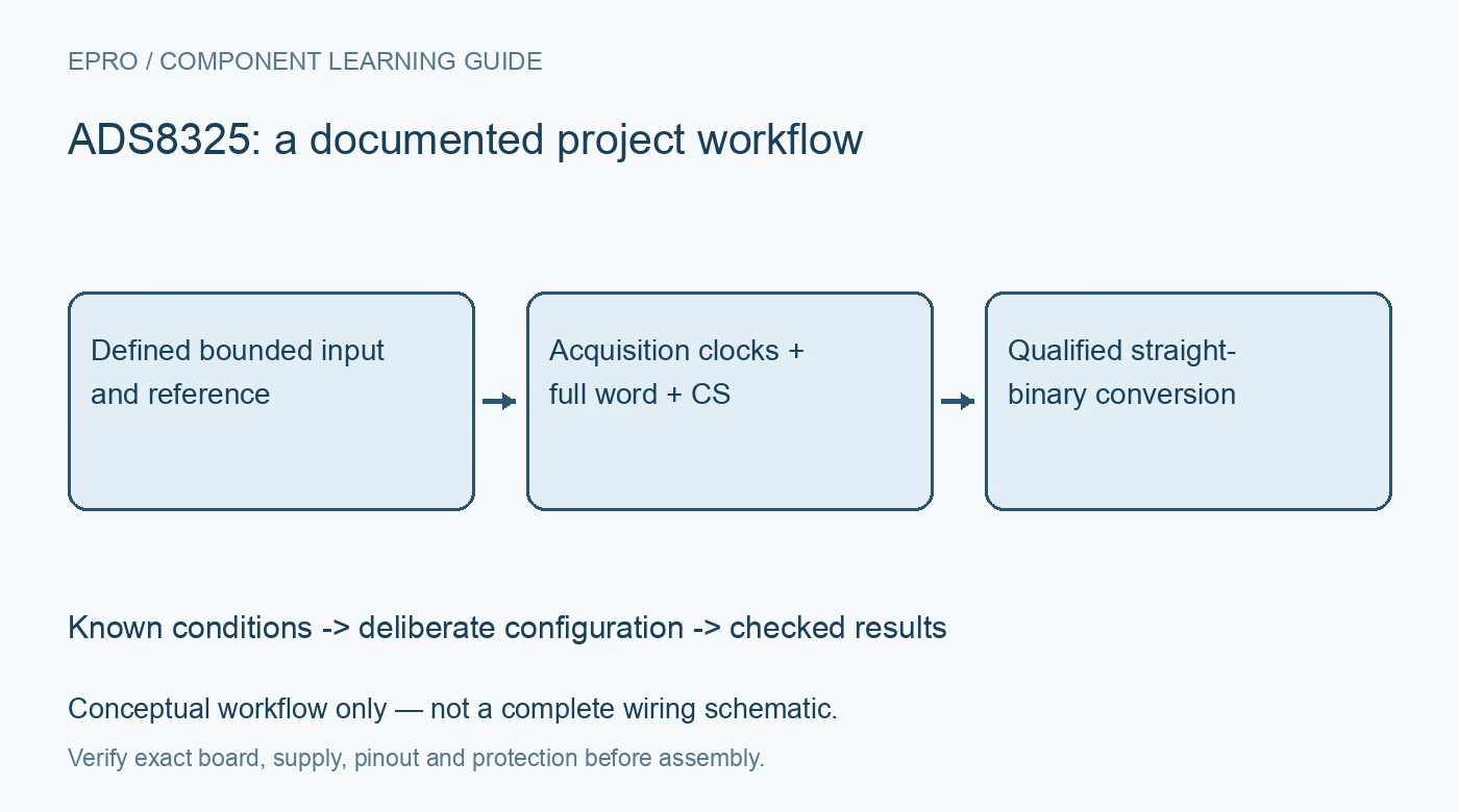
ADS8325 SAR ADC: 7 Checks for Input Limits and Complete Frames
Read ADS8325 conversions with seven checks for restricted negative-input range, reference drive, acquisition clocks, full serial frames and unsigned scaling. This is a documentation-based planning guide, not a report of independent hands-on testing.
1. Review the supply and reference together
ADS8325 is a sixteen-bit SAR converter operating across its specified 2.7 V to 5.5 V supply range. Its external reference has a documented lower limit of 2.5 V and must remain compatible with the supply and pin constraints. Do not lower the reference arbitrarily to obtain smaller nominal steps. Provide appropriate bypassing and verify the logic thresholds at the actual supply. Similar pinouts to older converters are useful for comparison, but are not a substitute for this part’s specifications. Manufacturer documentation.
2. Understand the restricted negative input
The input difference is captured between +IN and minus-IN, but the negative input is restricted to approximately minus 0.3 V through plus 0.5 V under the documented conditions. This is not a fully differential input centered anywhere between the supply rails. Use the negative pin for the intended near-ground sensing or common-mode rejection arrangement and check both individual pin limits. A sensor with a large common-mode voltage needs suitable conditioning rather than a signed software cast. Manufacturer documentation.
3. Budget acquisition time and source impedance
The switched-capacitor input must settle from the connected source during acquisition. Source resistance, filter capacitance and input step size all affect the result. Review the sampling interval and reference drive against the intended clock rate before relying on a stable-looking code. The reference also supplies dynamic conversion demand, so a correct DC voltage alone does not demonstrate adequate performance. Begin with a known bounded low-impedance source and then qualify the actual sensor and filter network. Manufacturer documentation.
4. Use the CS and clock sequence from the timing diagram
A new conversion requires the documented CS/SHDN high-to-low sequence, with conversion progression tied to DCLOCK. The interface needs at least twenty-two clock cycles for a complete sixteen-bit conversion; the example twenty-four-clock sequence is convenient for byte-oriented controllers. Do not read only sixteen clocks and assume every received bit is conversion data. Account for the initial acquisition and output timing, then check bit alignment against known input values and a logic trace. Manufacturer documentation.
Newest in the store


5. End each frame deliberately rather than free-running CS
Keeping CS low after the result does not start a fresh conversion automatically. The documented behavior can repeat data in a different bit order before subsequent output behavior changes. Use an explicit complete frame and restore CS high before requesting another result. Avoid depending on extra clocks outside the selected timing diagram. An accidental repeated word can appear exceptionally quiet, so pair received data with a verified conversion request rather than interpreting low variation as evidence of measurement quality. Manufacturer documentation.
6. Apply straight-binary scaling without signed reinterpretation
The conversion result uses straight binary for the documented unipolar differential span. With the allowed input arrangement, calculate nominal voltage from code times VREF divided by 65536, then consider offset and gain errors separately. Zero, midpoint and near-full-scale tests should produce the expected unsigned ordering. Sign-extending bit fifteen would incorrectly turn the upper half of the input span negative. Preserve raw bytes and alignment diagnostics so framing mistakes remain distinguishable from an analog overrange. Manufacturer documentation.
7. Verify restart, throughput and measurement freshness
Exercise conversion requests at conservative speed first, then qualify the intended rate with the real source and reference. Record CS timing, clock count, raw word and timestamp with the accepted samples. Check startup and shutdown-to-active behavior instead of assuming a bus transaction guarantees analog readiness. Compare repeated known levels and bounded steps, marking incomplete frames or inadequate settling as invalid. Nominal sixteen-bit resolution does not guarantee sixteen-bit useful accuracy once reference noise, source settling and board layout are included. Manufacturer documentation.
Related reading: ADS8320 SAR ADC: 7 Checks for Input Limits and Clock Frames.
Catalog note: The exact-part search did not return a matching Epro listing during preparation. Check the current catalog; this guide makes no price, availability or included-accessory claim.