


ADS8344 ADC: 7 Checks for Input Pairs and Serial Clocking

ADS8344 ADC: 7 Checks for Input Pairs and Serial Clocking
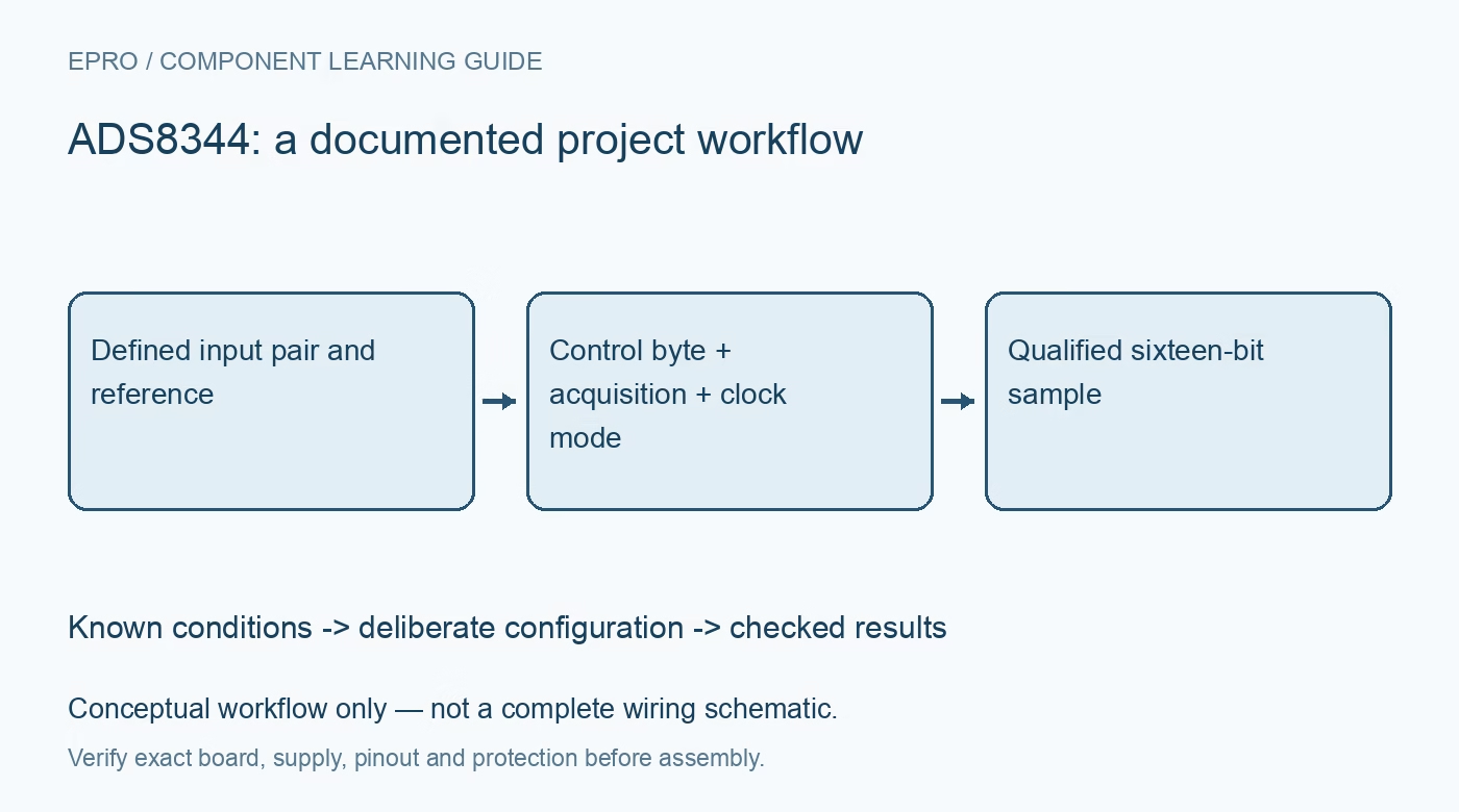
Plan ADS8344 acquisition with seven checks for input-pair mapping, unipolar coding, control bytes, clock modes, reference settling and complete serial frames. This is a documentation-based planning guide, not a report of independent hands-on testing.
1. Choose the input topology before the command
The ADS8344 supports eight single-ended channels or four differential channel pairs, selected through its control byte. Use the datasheet channel tables to identify the actual positive and negative inputs; an address number alone is not a complete analog route description. In single-ended mode, the measurement is referenced to COM. Record the selected topology and board connections together so the software cannot silently interpret a different pair as the same physical sensor. Manufacturer documentation.
2. Keep differential operation distinct from bipolar coding
The converter uses straight-binary output for the documented unipolar differential range. Differential capability does not mean arbitrary negative input differences produce signed two’s-complement data. Check both individual pin limits and the allowed difference against the reference and supply. If a sensor swings around zero, design the required conditioning rather than casting the received word to a signed integer. Validate polarity with known bounded voltages before connecting the signal source used in normal operation. Manufacturer documentation.
3. Drive acquisition and reference nodes deliberately
The sampling network needs time to charge from the selected source. Source impedance, filtering and a large channel-to-channel voltage step can all affect settling. Review acquisition timing and reference-drive requirements under the actual supply and sampling rate, including the relevant electrical-characteristics conditions. A reference with a correct DC voltmeter reading may still respond poorly to dynamic demand. Use a stable known source first and inspect repeated readings after switching between substantially different channel voltages. Manufacturer documentation.
4. Build the complete control byte
The start bit must be high, the channel-selection bits must match the intended input mapping, and the single-ended or differential selection must be explicit. The final power and clock-mode bits also change behavior; do not reuse a constant from an unrelated ADC. Save the transmitted byte in a diagnostic record next to the returned conversion. Test at least two distinct channels with intentionally different voltages, making command-order errors easier to distinguish from analog noise or offset. Manufacturer documentation.
Newest in the store


5. Select one documented clock-mode sequence
Internal-clock and external-clock operation require different handling of conversion timing and BUSY. The clock-mode selection is part of the command, not merely a controller SPI setting. Use one complete manufacturer timing diagram as the initial implementation and verify the corresponding CS, DCLK, DIN, DOUT and BUSY behavior. Do not splice a BUSY rule from one mode into a frame from the other. Treat shutdown and wake behavior as additional states requiring explicit qualification. Manufacturer documentation.
6. Capture all sixteen bits including the final bit
The high-throughput sequence overlaps the next command to achieve twenty-four clock cycles per conversion. With a byte-oriented controller, the last conversion bit needs particular care; the documented thirty-two-clock approach is another option. Simply receiving three bytes does not prove the entire result has been captured. Check bit alignment using known patterns and verify the final bit on a logic trace. Keep the required acquisition interval even if the serial transfer itself is clocked faster. Manufacturer documentation.
7. Preserve channel and timing identity in results
Log the command, input pair, reference, clock mode, raw word and timestamp for each accepted reading. Begin with grounded or known bounded test inputs, then exercise channel changes and different source impedances. Compare a conservative transfer sequence with any optimized overlapping sequence before adopting the latter. A stable number without route identity is not a reliable measurement record. Flag incomplete frames or unqualified settling instead of recycling the last plausible value as though it were new data. Manufacturer documentation.
Related reading: ADS8332 Multiplexed ADC: 7 Checks for Acquisition and Channel Tags.
Catalog note: The exact-part search did not return a matching Epro listing during preparation. Check the current catalog; this guide makes no price, availability or included-accessory claim.