


INA253 Integrated-Shunt Monitor: 7 Checks for References and Thermal Limits

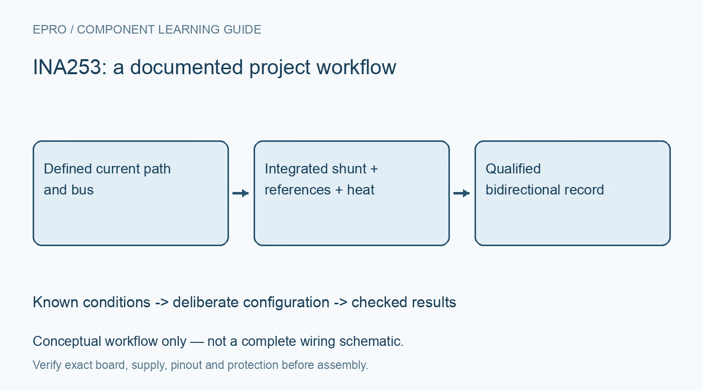
INA253 Integrated-Shunt Monitor: 7 Checks for References and Thermal Limits
Plan INA253 bidirectional current sensing with integrated-shunt routing, gain selection, reference bias, PWM sampling and thermal derating. This is a documentation-based planning guide, not a report of independent hands-on testing.
1. Distinguish the power path from the Kelvin signal path
INA253 combines a current-sense amplifier with a precision two-milliohm shunt. The IS terminals carry load current, while SH and IN connections provide the Kelvin sensing and optional filtering arrangement described by the manufacturer. Follow every required power-pin connection and the exact pin table, including reserved and do-not-connect pins. Do not route load current through small signal traces or assume every NC label has identical instructions. The integrated resistor simplifies sensing but does not eliminate careful PCB current routing. Manufacturer documentation.
2. Select the gain in millivolts per ampere
The gain options are 100 mV/A, 200 mV/A and 400 mV/A for the respective suffixes. These are complete current-to-output sensitivities with the integrated shunt, not ordinary amplifier gains to multiply by an additional external shunt value. Verify marking and firmware scaling together. For a given supply and reference midpoint, higher sensitivity reduces the available current range before clipping. A device capable of carrying a current thermally may still be unable to represent that current within the selected output range. Manufacturer documentation.
3. Separate the bus range from the low-voltage supply
The amplifier operates from a 2.7 V to 5.5 V supply with a documented common-mode range from negative 4 V to positive 80 V. Those are different quantities. Check input and signal-pin limits and output compatibility with the ADC independently of bus voltage. The device provides no galvanic isolation. Use protected low-energy testing initially and choose instruments appropriate to the installation rather than treating the high common-mode rating as a guarantee that arbitrary grounding or fault conditions are safe. Manufacturer documentation.
4. Drive both reference pins deliberately
REF1 and REF2 set the output baseline through the internal reference network. For symmetrical bidirectional measurement, a suitable midpoint provides room for positive and negative excursions. The reference inputs must stay between ground and VS and should use the documented low-impedance connections. Do not leave one floating or assume a high-impedance divider behaves like an ideal voltage source. Include reference accuracy and movement in the current calculation, and measure the actual zero-current baseline before applying a gain-only conversion. Manufacturer documentation.
Newest in the store


5. Use package loss and layout in the thermal budget
The sensing element is two milliohms, but the datasheet identifies approximately 4.5 milliohms of total package resistance for heat generation. Current-squared-resistance dissipation must therefore use the relevant full path, not the shunt alone. The fifteen-amp continuous headline depends on copper, airflow and ambient conditions; the manufacturer shows derating to ten amperes at 125 degrees Celsius for the specified one-ounce, no-airflow condition. Better cooling examples do not automatically transfer to a small breakout board. Manufacturer documentation.
6. Qualify PWM rejection and acquisition timing
Enhanced PWM rejection helps when common mode changes rapidly, but it does not guarantee a valid instantaneous sample at every switching edge. Include settling, bandwidth, external filtering and ADC acquisition in the timing plan. Check output swing and loading at both current extremes and preserve clipped or transient-invalid readings. The integrated low-inductance shunt still has a finite response during fast current changes. Distinguish electrical settling from real load-current dynamics before choosing a sampling delay or filtering algorithm. Manufacturer documentation.
7. Validate signed current with a traceable load sequence
Apply known bounded currents in both directions and compare output, reference baseline and the independent current measurement. Repeat near the smallest useful current and the intended thermal load while monitoring device and copper temperature. Record gain suffix, supply, reference connections, layout, filtering and sampling timing. Retain overload or saturation as invalid states rather than smoothing them into plausible data. This documentation-based plan does not claim independent accuracy testing or establish safe continuous current for an untested board. Manufacturer documentation.
Related reading: INA241A Current-Sense Amplifier: 7 Checks for Dual References and PWM Sampling.
Catalog note: The exact-part search did not return a matching Epro listing during preparation. Check the current catalog; this guide makes no price, availability or included-accessory claim.