


W25Q32JV Flash: 7 Voltage and Erase-Geometry Checks

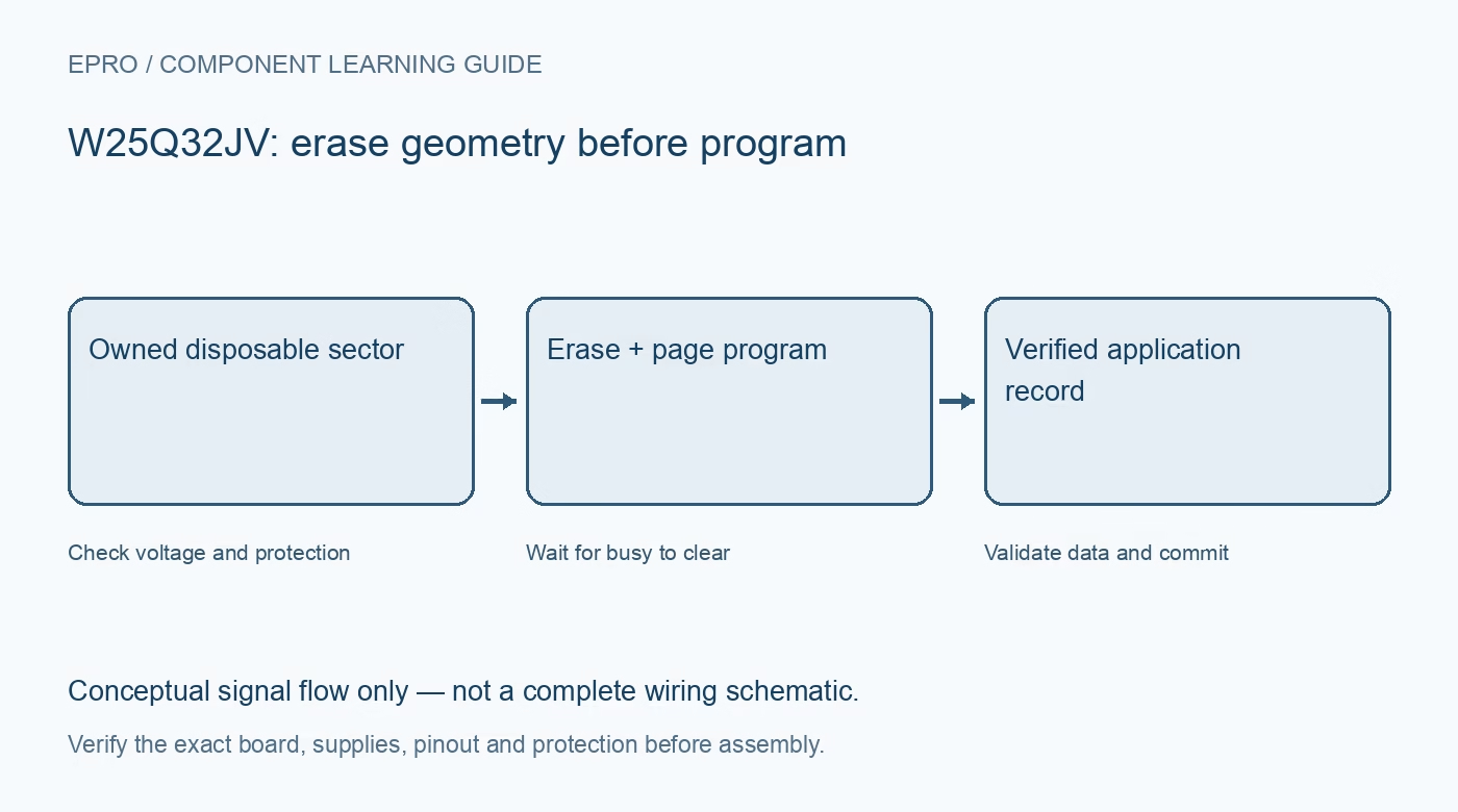
W25Q32 names a thirty-two-megabit flash family, not a universal voltage or command configuration. This guide specifically references W25Q32JV documentation. Its four-megabyte array is useful for storage, but programming and erasing require a different design from byte-rewritable EEPROM or RAM.
Read the complete device suffix
Verify JV and the exact package and ordering code before applying voltage and interface limits. Other family variants can differ. The referenced JV operates from 2.7 V to 3.6 V; it is not a five-volt chip merely because an Arduino or programmer supplies five volts at another connector.
Separate capacity from address width
Thirty-two megabits equals four megabytes, with addresses covering the documented array. A driver must use the correct command and address format rather than assuming every SPI flash has the same capacity or address mode. Keep bounds checks around reads, writes and any erase operation.
Plan erase units before allocating records
The array supports four-kilobyte sectors and larger documented erase units. Erasing a sector removes all its contents, not just one updated setting. Allocate data so that an application can preserve unrelated records, and reserve a separate disposable test sector instead of experimenting on an existing firmware image.
Treat page programming as a bounded operation
A page-program transaction handles up to 256 bytes within the current page. Starting near the end leaves fewer bytes available. Crossing the page boundary wraps within that page rather than continuing safely to the next. Software must split transfers by the remaining page length.
Understand erased and programmed states
Programming is intended for erased locations and changes bits toward their programmed state; it is not arbitrary in-place byte replacement. Restoring erased bits requires an appropriate erase operation. A file system or record layer must handle this geometry instead of assuming repeated writes behave like ordinary RAM assignments.
Check protection, write-enable and busy state
A write-enable command and correct protection configuration are prerequisites, not proof of completion. Status identifies whether the device is busy and whether write enable is latched. Review the exact protection scheme before changing it; indiscriminately clearing security or lock settings can damage an existing application’s assumptions.
Newest in the store


Design recovery and electrical access safely
Use compatible logic levels and a documented standalone connection. Do not attach a programmer to a powered target with competing bus drivers or assume an in-circuit clip is electrically safe. Plan power-loss-safe records and verify data after completed operations; successful SPI traffic alone does not prove durable, correct storage.
Frequently asked questions
Is W25Q32 a thirty-two-megabyte device?
No. Thirty-two megabits equals four megabytes.
Can one byte be erased without affecting its sector?
Not through a sector erase; the application must preserve or relocate other data in that erase unit.
Availability and illustration note
No matching Epro product was returned by the catalog search on 21 October 2026 UTC. This learning guide does not assert stock, a selling price or compatibility of an unidentified substitute. The illustration is an original conceptual signal-flow diagram, not a product photograph or complete wiring schematic.
Related Epro reading
For a first bench setup, review breadboard connections and continuity checks and I2C voltage-level translation. These guides do not replace the exact module schematic.
Technical references and limitations
Source: Winbond W25Q32JV Revision J datasheet. Electrical limits apply to the named part, not automatically to every carrier board. This is a documentation-based learning workflow, not a claim of independent hardware testing, traceable calibration or safety certification.