


PCF8591 ADC and DAC: What an 8-Bit I2C Module Can Do

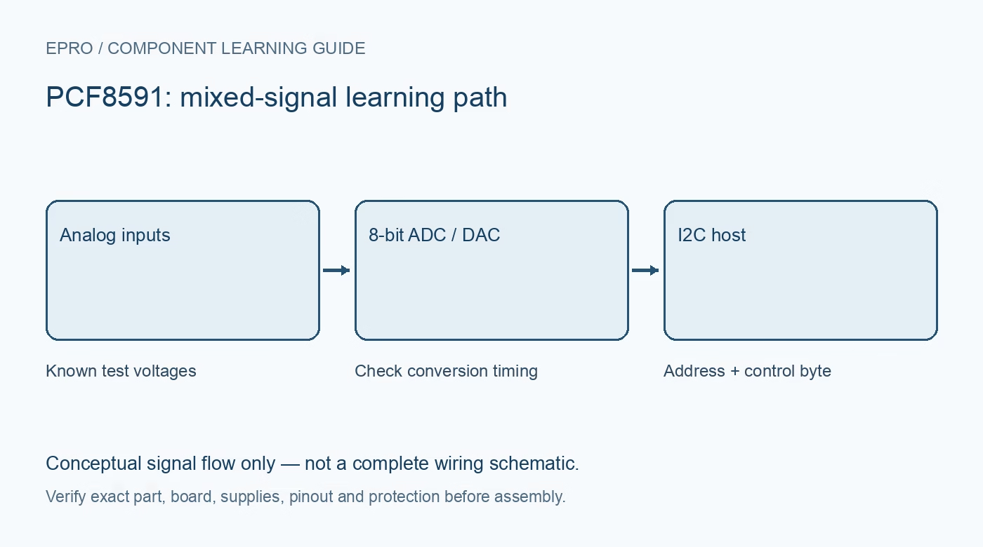
PCF8591 combines an 8-bit analog-to-digital converter and an analog output behind an I2C interface. It is useful for learning mixed-signal communication, but its resolution, conversion sequence and carrier-board extras must be understood before calling it a precision sensor interface.
Read the converter rather than the breakout photograph
The NXP device provides four analog inputs and one analog output with selectable input configurations. A carrier may add a potentiometer, light-dependent resistor or thermistor. Those are board-specific extras, not intrinsic calibrated measurement functions of the PCF8591. Identify which jumpers connect them before attaching an external source.
Check the power and bus levels
The chip datasheet specifies its supply range, but the complete module may impose additional restrictions. I2C pull-ups on a 5 V carrier can expose a 3.3 V host to an excessive voltage. Check where every pull-up is connected and provide appropriate bus-level adaptation or a fully compatible supply arrangement. A responding address does not prove electrical compliance.
Understand eight-bit granularity
An eight-bit conversion uses 256 ideal code positions. Reference, supply noise, converter errors and source conditions limit actual measurement quality. A temperature inferred from an undocumented thermistor is not calibrated merely because the serial output prints decimals. Keep raw values and the assumed conversion model in the test record.
Account for the previous conversion byte
NXP documents that the first byte in a read cycle contains the result of the previous conversion; after power-on reset that first code is 0x80. Software must account for this pipeline, particularly after selecting a channel. Ignoring it can create plausible but shifted channel readings that are difficult to diagnose from a changing sensor alone.
Use the analog output as a signal, not a power source
The DAC output is intended for a compatible signal load within its documented limits. It is not a supply rail for motors, lamps or arbitrary electronics. Enable and configure it correctly, allow settling and measure with a suitable high-impedance instrument. The output does not automatically reach every ideal endpoint under all loading conditions.
Choose a different converter when requirements demand it
If the project needs finer resolution, higher throughput, simultaneous sampling or guaranteed precision, compare converters against those specific requirements. Do not treat a low-cost learning board as equivalent to a calibrated data-acquisition instrument. For the PCF8591, clean low-voltage inputs and correct transaction timing are more useful than unsupported claims of high precision.Newest in the store


Availability and illustration note
No matching product was found in the checked Epro catalog for this topic on 19 October 2026. This article therefore does not quote an Epro price or claim stock. The original illustration shows conceptual signal flow only, not a complete circuit or a photograph of a supplied product. Obtain a documented component or carrier with a known pinout and electrical specification.
Frequently asked questions
Why can the first byte belong to another channel?
The first transmitted read byte contains the previous conversion result. The driver must handle the documented conversion pipeline.
Can the DAC output power another board?
No. Treat it as a limited analog signal output and check its specified loading requirements.
Related Epro reading
Review breadboard connections before assembling a prototype. For controller expansion, the Mega 2560 pin guide explains why pin names and electrical limits must be checked together.
Technical references and test limitations
This guide uses the documentation linked below. The procedures are for a controlled, low-voltage learning setup; no independent hands-on test of the particular seller board is claimed. Record the actual part markings, wiring and firmware version before drawing conclusions from a test.