


ADS1015 ADC: 7 Range and Multiplexer Checks

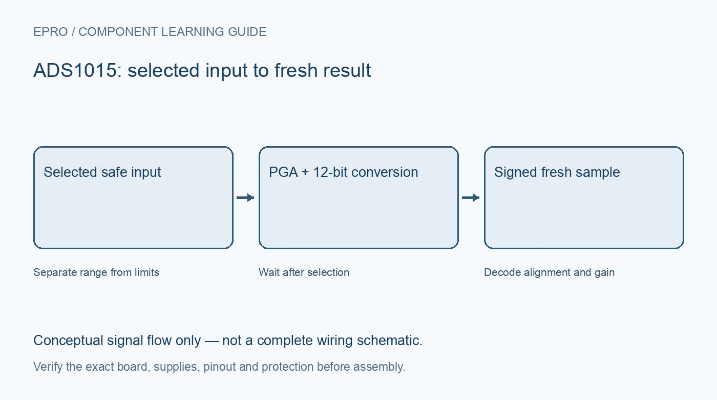
An ADS1015 is a twelve-bit I2C ADC with a programmable input range and channel multiplexer. It is not a faster sixteen-bit ADS1115, and a wide numeric full-scale setting does not make its input pins tolerant of arbitrary voltages. Select the signal network and conversion schedule together.
Distinguish ADS1015 from ADS1115
The similar family devices use different resolution and maximum data rates. ADS1015 provides twelve-bit results at rates up to 3300 samples per second; ADS1115 is a different sixteen-bit converter. Use the correct driver model rather than assuming a shared register layout guarantees identical voltage scaling.
Keep input rails separate from full scale
The programmable differential range can extend numerically to plus or minus 6.144 V, but normal absolute input voltages are still constrained by the device supply rails. A 3.3 V-powered ADC cannot safely measure a 6 V pin voltage simply because software selects the widest range.
Understand the shared converter
The ADS1015 supports four single-ended selections or suitable differential pairs through a multiplexer. It does not sample four channels simultaneously. Plan aggregate conversion time, channel-switch behaviour and source settling before interpreting a multi-channel scan as a set of observations taken at one instant.
Select gain for the actual signal
A narrower full-scale setting gives a smaller voltage step but less differential headroom. Include offset, expected excursions and noise before choosing it. An input that clips numerically is not repaired by a later software multiplier, and a valid negative differential does not permit a negative absolute pin voltage.
Review source impedance and acquisition
The ADC input structure and selected range affect loading. A high-resistance sensor network may need buffering or a different acquisition design. Verify the complete source, filtering and conversion mode rather than assuming every I2C ADC input behaves like an ideal infinite-resistance voltmeter.
Plan address and alert connections
The device offers four pin-selected I2C addresses and a programmable comparator or ready-related output function. Check the physical address connection, pull-up rail and exact mode before using ALERT/RDY. A configurable logic output is not automatically a calibrated protective cutoff.
Newest in the store


Keep resolution distinct from system accuracy
Reference error, input error, gain setting, noise and the external network all contribute to uncertainty. Start with known safe low-voltage sources and document the intended operating point. This guide does not establish traceable calibration or medical measurement suitability.
Frequently asked questions
Does the widest range make the inputs 6 V tolerant on a 3.3 V supply?
No. Absolute input operating limits remain tied to the supply rails.
Are all four channels converted at the same instant?
No. They share a multiplexed converter and need a deliberate scan schedule.
Availability and illustration note
No matching Epro product was returned by the catalog search on 21 October 2026 UTC. This learning guide does not assert stock, a selling price or compatibility of an unidentified substitute. The illustration is an original conceptual signal-flow diagram, not a product photograph or complete wiring schematic.
Related Epro reading
For a first bench setup, review breadboard connections and continuity checks and I2C voltage-level translation. These guides do not replace the exact module schematic.
Technical references and limitations
Source: Texas Instruments ADS101x ADC datasheet. Electrical limits apply to the named part, not automatically to every carrier board. This is a documentation-based learning workflow, not a claim of independent hardware testing, traceable calibration or safety certification.