


ADS1220 ADC: 7 PGA and Reference Selection Checks

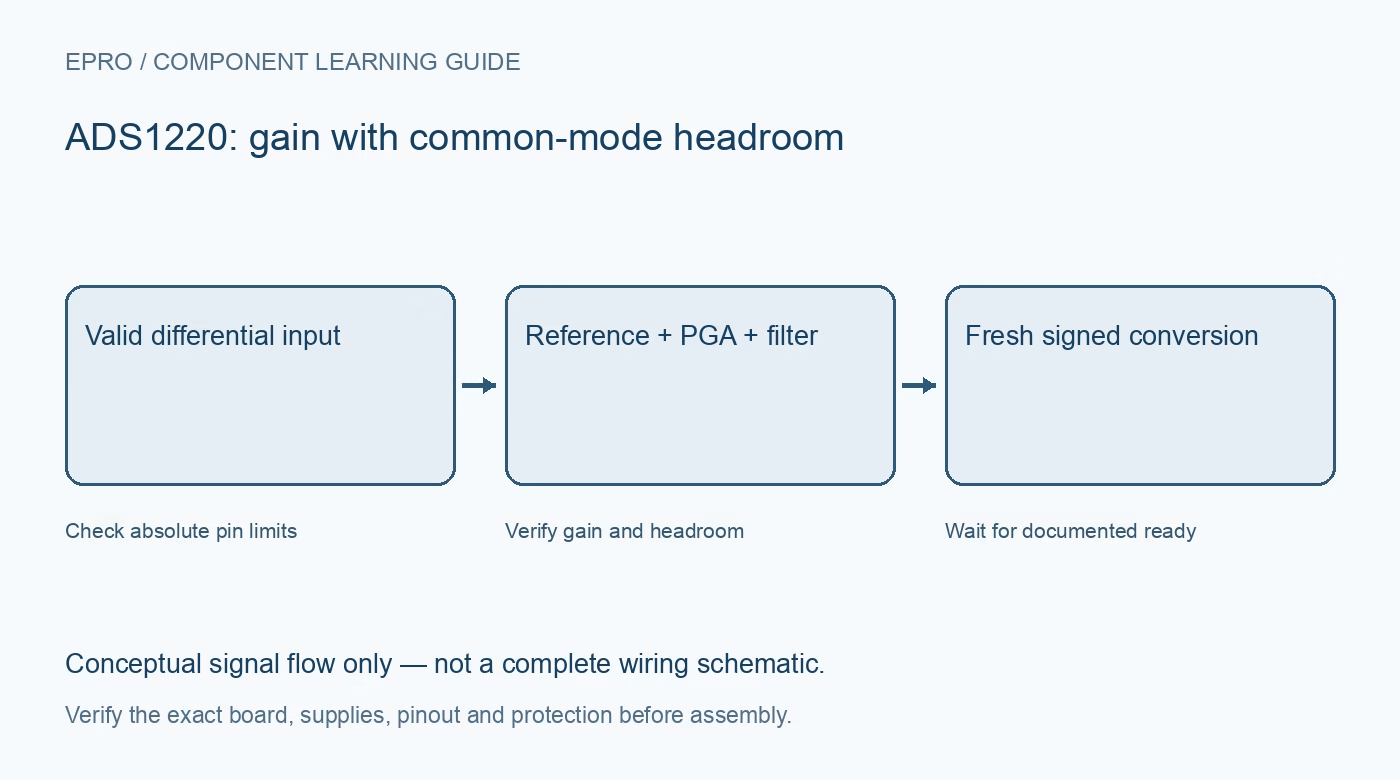
An ADS1220 is a multiplexed delta-sigma converter for low-level measurements. Its resolution label does not guarantee twenty-four useful bits from an arbitrary sensor board. Start with a defined signal range, reference and wiring arrangement before selecting gain or a carrier for a low-voltage bench project.
Identify the exact board and supplies
The chip and a breakout are different assemblies. Read the carrier schematic for analog and digital supply connections, reference routing, decoupling and any fitted resistors. A board that exposes four analog inputs does not contain four independent simultaneous converters. The multiplexer feeds one conversion path.
Choose differential range deliberately
The nominal differential full-scale range depends on reference voltage divided by PGA gain. The internal reference is nominally 2.048 V, but an external-reference design needs its own valid source and routing. A numeric differential span is not permission for either physical input to exceed its allowed absolute voltage.
Check PGA common-mode headroom
An enabled PGA requires headroom at both inputs, with limits that depend on supply, gain and signal amplitude. Simply grounding the negative input at high gain can violate those conditions. Check the datasheet common-mode equations at the worst intended signal rather than using differential range alone.
Distinguish bypass from high-gain operation
PGA bypass is available only with supported low gains of one, two or four. It changes the input restrictions and can suit an appropriate ground-referenced measurement. It is not a universal solution that preserves high-gain PGA behavior. Confirm the actual configuration and keep normal signals inside the supply rails.
Select conversion mode and rejection together
Data rate depends on normal, duty-cycle or turbo mode. The headline maximum rate is not the setting for every precision application. Check the specified filter and clock conditions for mains-frequency rejection; selecting an arbitrary rate does not automatically reject both 50 Hz and 60 Hz interference.
Plan excitation as a separate circuit
The programmable current sources can support sensor excitation, but compliance, reference generation and lead resistance still require a complete design. Do not connect an unidentified probe and assume automatic temperature accuracy. Begin with protected low-voltage test sources before adding a bridge or resistance measurement network.
Newest in the store


Specify the digital interface and evidence
ADS1220 uses SPI mode one, not whichever mode another converter happened to use. Plan chip select, clock and ready signaling before assembly. Acceptance should include correct identification, configuration readback, fresh signed conversions and plausible scaling, not a claim of traceable calibration based on a stable printed number.
Frequently asked questions
Are all four inputs sampled at once?
No. The inputs are multiplexed into one conversion path.
Does 24-bit output guarantee 24-bit accuracy?
No. Noise, reference error, gain, wiring and settling determine useful measurement performance.
Availability and illustration note
No matching Epro product was returned by the catalog search on 21 October 2026 UTC. This learning guide does not assert stock, a selling price or compatibility of an unidentified substitute. The illustration is an original conceptual signal-flow diagram, not a product photograph or complete wiring schematic.
Related Epro reading
For a first bench setup, review breadboard connections and continuity checks and I2C voltage-level translation. These guides do not replace the exact module schematic.
Technical references and limitations
Source: Texas Instruments ADS1220 datasheet. Electrical limits apply to the named part, not automatically to every carrier board. This is a documentation-based learning workflow, not a claim of independent hardware testing, traceable calibration or safety certification.