


ADS7057 SAR ADC: 7 Checks for Differential Samples at Speed

ADS7057 SAR ADC: 7 Checks for Differential Samples at Speed
Check ADS7057 input common mode, offset calibration, acquisition timing and previous-frame data before interpreting high-speed samples. This is a documentation-based planning guide, not a report of independent hands-on testing.
1. Specify both input voltages, not only their difference
The ADS7057 is a fourteen-bit SAR converter with throughput up to 2.5 MSPS under its specified timing conditions. Its differential range is plus or minus AVDD, but that does not permit arbitrary negative pin voltages. Document AINP, AINM and their average across the complete waveform. The recommended common mode is tightly centered around half AVDD. A differential signal that appears valid mathematically can still violate an individual input or common-mode requirement and produce misleading conversion results. Manufacturer documentation.
2. Treat AVDD as part of the measurement reference
The analog supply sets the conversion range, so supply error and noise affect voltage interpretation. AVDD operates from 2.35 V to 3.6 V, while DVDD can operate independently from 1.65 V to 3.6 V. Keep those limits distinct when choosing controller logic and analog drive circuitry. Review decoupling and return placement in the reference layout. Record the measured analog supply with each characterization run rather than assuming the nominal regulator label is an exact calibration reference. Manufacturer documentation.
3. Design the source for the acquisition interval
A switched-capacitor input requires the source and any filter to settle during acquisition. Low sample rate does not automatically excuse a slow or high-impedance driver if the chosen transaction leaves too little acquisition time. The datasheet specifies a minimum acquisition interval of 95 ns for the relevant timing sequence. Include source impedance, amplifier settling, filter capacitance and board parasitics in the assessment. Start with a bounded, stable source and compare settled codes before introducing a fast-changing sensor waveform. Manufacturer documentation.
4. Separate startup calibration from ordinary conversion
At power-up, the host must provide the documented twenty-four-clock first transaction to perform offset calibration. During normal operation, the calibration sequence uses sixty-four clocks instead. These are not interchangeable with an ordinary conversion frame. Incomplete sequences can abort calibration, so inspect chip-select behavior as well as the number of clocks. Mark calibration intervals as nonmeasurement records and provide the required acquisition time afterward. A successful SPI transfer alone does not establish that the converter completed the intended internal state transition. Manufacturer documentation.
Newest in the store


5. Account for the previous-sample serial pipeline
An ordinary conversion requires at least eighteen SCLK falling edges. The data shifted out belong to the previous conversion, with a leading zero and the documented fourteen-bit arrangement. The first transferred data after power-up are zeros rather than an established measurement. Build a timing sketch that labels the analog sampling edge, conversion number and output frame number. Test the unpacking code using deliberately different input levels so a one-frame association error cannot survive behind an apparently stable DC reading. Manufacturer documentation.
6. Preserve signed codes and reject bad transactions
Apply the manufacturer transfer function to the fourteen-bit conversion result and its two’s-complement representation. Keep framing bits separate before sign extension; blindly casting a wider SPI word can change polarity or scale. Store the supply reference and sample sequence number with the interpreted value. This simple interface does not make host timeouts or incomplete frames valid data. Use explicit software quality flags and a known-input check rather than inventing a converter CRC or accepting the last buffer contents after an error. Manufacturer documentation.
7. Increase throughput only after a bounded baseline passes
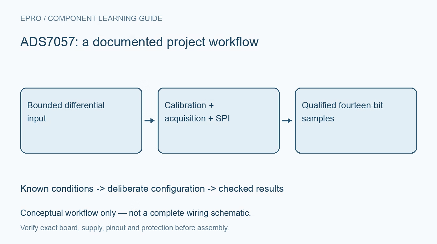
Begin with documented supplies, a quiet DC source and generous timing. Compare zero differential and small positive and negative differential inputs while maintaining the required common mode. Then increase clock and sampling rate within the tables, watching for settling error, supply disturbance and sample association mistakes. Retain raw words alongside calculated voltage and timing settings. The final useful result is a qualified acquisition path under recorded conditions, not a claim that every board delivers datasheet resolution at its headline maximum speed. Manufacturer documentation.
Related reading: ADS7054 SAR ADC: 7 Checks for Differential Sampling and Calibration.
Catalog note: The exact-part search did not return a matching Epro listing during preparation. Check the current catalog; this guide makes no price, availability or included-accessory claim.