


DAC8811 Multiplying DAC: 7 Checks for I-to-V Output and Updates

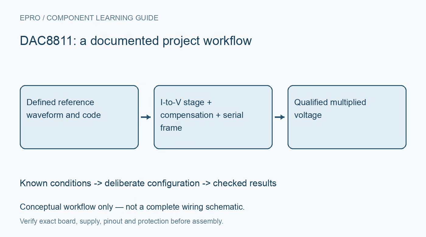
DAC8811 Multiplying DAC: 7 Checks for I-to-V Output and Updates
Design a DAC8811 multiplying-DAC stage with seven checks for current output, external I-to-V feedback, reference polarity, compensation and serial updates. This is a documentation-based planning guide, not a report of independent hands-on testing.
1. Identify a multiplying current-output converter
DAC8811 is a sixteen-bit multiplying DAC, not a complete buffered voltage-output source. Its reference establishes the current scale, and an external transimpedance amplifier normally converts that current to a useful voltage. The device supplies an internally matched feedback resistor through RFB for the documented topology. Begin from that circuit rather than connecting IOUT as though it were a low-impedance voltage pin. Record the amplifier, supply rails and reference arrangement as part of the converter design. Manufacturer documentation.
2. Calculate output sign as well as magnitude
In the standard inverting I-to-V arrangement using the matched feedback path, the ideal output is proportional to minus VREF times code divided by 65536. A positive reference therefore produces a negative output in that topology. Check amplifier supply headroom before assuming a single positive rail can deliver it. Midscale is not inherently zero voltage, and full-scale code is one step short of the ideal endpoint. Added offset or bipolar stages require their own resistor and error analysis. Manufacturer documentation.
3. Separate reference range from the digital supply
The DAC supply operates from 2.7 V to 5.5 V, while the reference input supports the documented positive and negative reference range, including multiplying applications. Those capabilities do not extend to arbitrary voltage on IOUT or the logic inputs. Review every pin’s operating limits and the reference source’s drive requirements. An AC reference also needs suitable bandwidth, distortion and slew performance in the surrounding analog chain; a multiplying feature does not make the entire stage frequency-independent. Manufacturer documentation.
4. Choose the amplifier around the summing node
Input offset, bias current, gain bandwidth and output swing all affect the I-to-V result. Keep the IOUT-to-inverting-input connection short and use the manufacturer feedback arrangement so parasitic capacitance remains controlled. Check the amplifier input and output conditions over reference polarity and code. The converter’s low supply current does not include the external amplifier or reference. Calculate total system power and noise rather than attributing a silicon-only headline to the completed analog-output channel. Manufacturer documentation.
Newest in the store


5. Design compensation for the actual layout
The DAC output capacitance, amplifier response and parasitic feedback paths can create peaking or instability. The datasheet discusses a small feedback compensation capacitor, with typical example values in the picofarad range. Treat those as design starting points, not a universal component value. Evaluate settling, overshoot and stability for the chosen amplifier, board and load. Increasing capacitance may reduce ringing while slowing response, so define the required error band and acquisition time before accepting the trade-off. Manufacturer documentation.
6. Update on the sixteenth rising clock edge
With CS low, the device shifts a sixteen-bit word on rising clock edges. The DAC update occurs on the sixteenth rising edge, not on a later rising CS edge as in some voltage DACs. Bring CS high for the required minimum interval before starting the next word. This distinction matters when synchronizing analog output to other devices. Check bit order, setup and hold timing with a trace, and keep incomplete words from being interpreted as a valid update sequence. Manufacturer documentation.
7. Validate gain, polarity and dynamic multiplication
Power-on reset sets the register to zero scale, but the complete amplifier and reference still need a controlled startup. Begin validation with a bounded DC reference and several codes, checking the expected output polarity and scaling. Then evaluate representative AC reference conditions if multiplication is required. Record code, reference waveform, output load, compensation and settling interval. Keep static calibration separate from dynamic distortion or bandwidth qualification; one accurate DC midpoint cannot certify a wideband multiplying application. Manufacturer documentation.
Related reading: DAC8830 Voltage DAC: 7 Checks for Unbuffered Output Accuracy.
Catalog note: The exact-part search did not return a matching Epro listing during preparation. Check the current catalog; this guide makes no price, availability or included-accessory claim.