


OPA197 ADC Driver: 7 Checks for Multiplexer Recovery and Settling

OPA197 ADC Driver: 7 Checks for Multiplexer Recovery and Settling
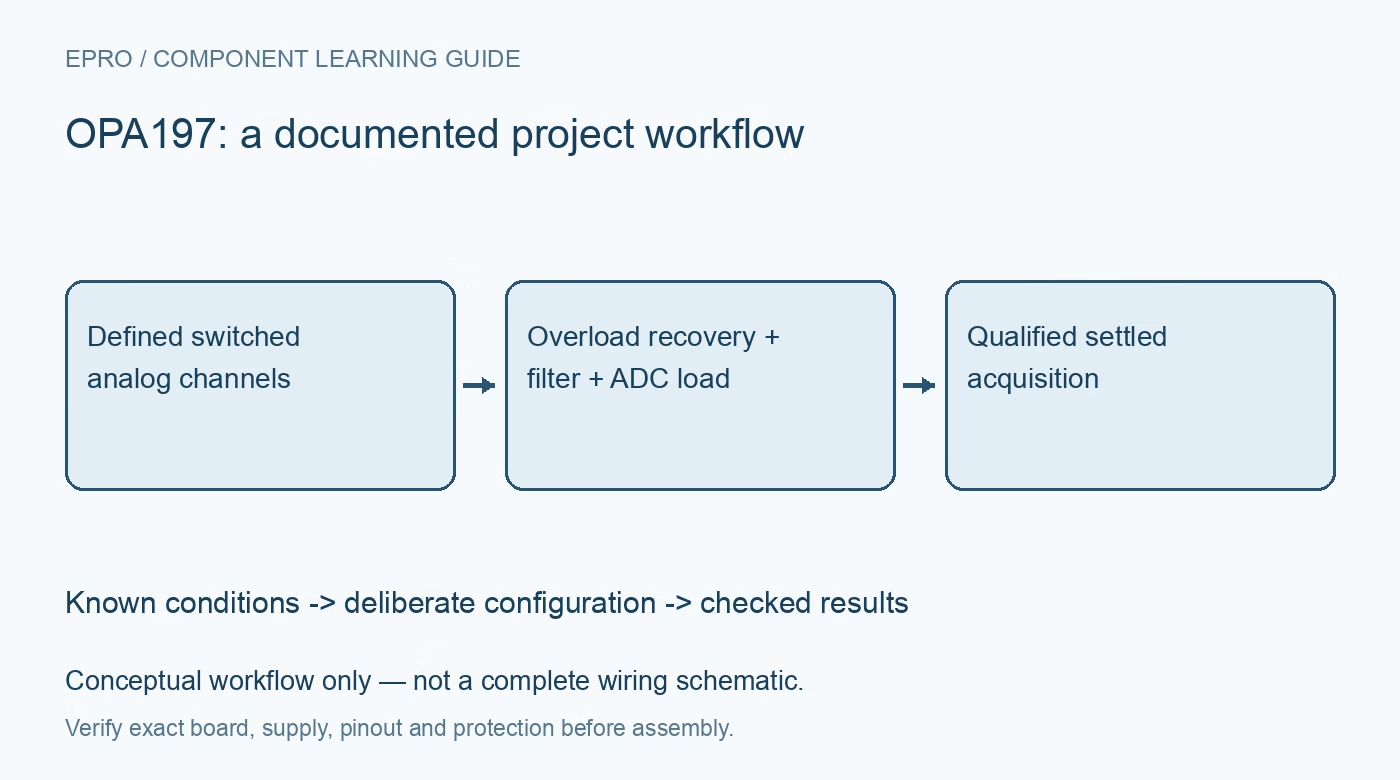
Plan an OPA197 multiplexed front end with differential-input protection behavior, full-step settling, ADC kickback control and load-dependent output headroom. This is a documentation-based planning guide, not a report of independent hands-on testing.
1. Define the largest switched-channel step
An amplifier after a multiplexer can see a nearly full-range step when adjacent channels have very different voltages. Specify that step, the scan rate and the ADC error target before choosing OPA197 as the driver. Check the documented 4.5 V to 36 V supply span, input range and required output range together. An op amp that accurately buffers a slowly varying bench voltage may still fail a rapid multiplexed acquisition schedule because its transient response and settling have not been evaluated. Manufacturer documentation.
2. Understand differential-input tolerance without ignoring pin limits
The manufacturer describes an input architecture that tolerates large differential voltages without the conventional back-to-back diode limitation of some precision amplifiers. This can help when a multiplexer changes channels faster than the output follows. It is not permission to exceed absolute input, supply or current ratings. Keep both physical input pins within their documented conditions during startup, normal operation and faults. A differential-voltage capability and an allowed common-mode range answer different questions about the same circuit. Manufacturer documentation.
3. Separate slew time, overload recovery and precision settling
The output may first slew toward a new level, recover from saturation if present, and then approach the final value within a small error band. These phases cannot be replaced by the 10 MHz gain-bandwidth headline alone. Use the relevant manufacturer curves and conditions to build an acquisition-time estimate, then measure the actual configuration. A fast edge or a crossing of the final voltage is not the same as settling to the resolution required by a high-resolution ADC. Manufacturer documentation.
4. Design the ADC input network as a dynamic load
A SAR ADC input can demand charge during acquisition, producing kickback that a static resistor load does not represent. Review driver output impedance, filter resistance, reservoir capacitance and acquisition timing together. The OPA197 capacitive-load capability is useful, but stability still depends on the exact loop and loading. Adding a large capacitor directly to the output can change phase margin and recovery. Use the manufacturer guidance and inspect both ringing and final settling with a suitable measurement setup. Manufacturer documentation.
Newest in the store


5. Check headroom at both output extremes
Rail-to-rail output does not reach either supply with zero error under every load. Include the ADC input range, filter voltage drop, output source or sink demand and common-mode conditions. If one channel drives the output into clipping, the next channel can inherit a recovery penalty. Evaluate the common-mode input-pair transition region for precision requirements as well. A one-point gain calibration cannot restore missing output headroom or remove a state-dependent error caused by the previous channel. Manufacturer documentation.
6. Keep layout and protection from corrupting the timing budget
Place supply bypassing close to the amplifier and keep feedback paths compact. Separate digital switching return currents from sensitive analog nodes, and evaluate leakage and capacitance introduced by protection components. A clamp chosen only for surge rating can load a high-impedance source or slow a channel transition. Thermal protection is not a normal accuracy feature; unexpected output interruption or heating deserves investigation. Document what happens when a channel connector is absent instead of relying on a floating input to settle conveniently. Manufacturer documentation.
7. Validate worst-case channel sequences rather than averages
Drive alternating low and high known inputs, then compare the first accepted sample after each switch with repeated samples after a longer dwell. Repeat with the intended ADC rate, filter and source impedances. Check startup, overrange recovery within ratings and output-load variation. Store channel order and timing alongside the measured error; average readings can conceal systematic first-sample contamination. This manufacturer-based guide provides a test strategy, not independent distortion, settling-time or sixteen-bit-system accuracy certification for the finished design. Manufacturer documentation.
Related reading: OPA2192 Precision Op Amp: 7 Checks for Rail-to-Rail Accuracy.
Catalog note: The exact-part search did not return a matching Epro listing during preparation. Check the current catalog; this guide makes no price, availability or included-accessory claim.