


TPS65023 PMIC: 7 Checks for Boot Defaults and DVS Completion

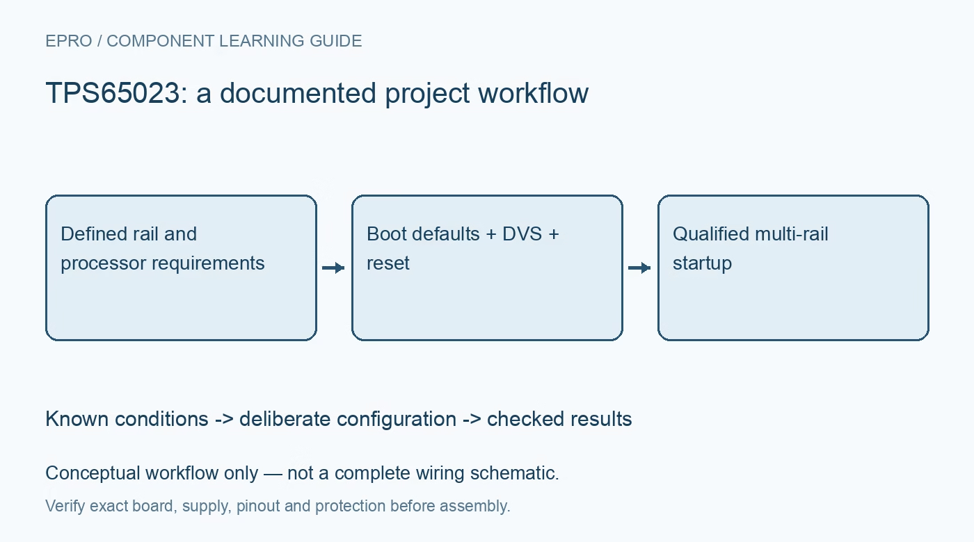
TPS65023 PMIC: 7 Checks for Boot Defaults and DVS Completion
Plan TPS65023 rails using their hardware defaults, enable paths, core-voltage ownership and reset behavior before trusting I2C or a cleared GO bit. This is a documentation-based planning guide, not a report of independent hands-on testing.
1. Build a rail map before configuring the PMIC
TPS65023 combines three step-down converters, general-purpose LDOs and a real-time-clock supply function. These rails have different capabilities and control paths; the device is not one interchangeable multi-output regulator. Confirm the exact TPS65023 or TPS65023B variant, board schematic and processor requirements. Record every load’s voltage, startup sequence, current and reset dependency. A working I2C connection does not establish that the processor is receiving safe default voltages before software begins to run. Manufacturer documentation.
2. Establish hardware-defined startup values first
The DEFDCDC and DEFLDO arrangements determine documented default rail behavior through their pin connections and applicable external networks. Follow the actual variant’s tables and equations rather than treating all default pins as generic digital inputs. Check the fitted straps and resistors before enabling a valuable processor. Software cannot repair an unsafe rail that is applied before the host has booted. Preserve the expected initial voltages and enable states independently of any later register settings. Manufacturer documentation.
3. Validate each converter and shared input demand
Select the inductors, bypassing and output networks according to each rail’s design guidance. Assess combined source demand, thermal dissipation and load transitions, not just the largest current figure in a family summary. A satisfactory reading on one rail does not qualify the others. Start with bounded test loads and a protected source. Keep switching loops and sensing returns consistent with the layout recommendations, and check the individual input connections and supply requirements rather than assuming all functions share one unrestricted pin. Manufacturer documentation.
4. Make core-voltage ownership explicit
The core-adjust control determines whether DCDC1 follows the documented hardware setting or the software-defined voltage. Its naming and bit polarity must be read carefully: do not infer the effect from an informal variable called adjustment-enabled. Follow the register procedure for selecting the target and transition rate, and verify the active control state. A written target value does not by itself prove that the output has changed or that a connected processor is prepared for that voltage transition. Manufacturer documentation.
Newest in the store


5. Do not confuse a cleared GO bit with regulation
The documented GO operation starts a transition toward the programmed core-voltage code. GO clears when the code transition completes, which is explicitly not the same as the physical rail having settled into regulation at the desired voltage. Respect the processor’s voltage and frequency sequencing requirements and qualify actual rail settling. Keep target code, transition state and measured voltage distinct in software and test logs. Do not release a consequential operating-state change solely because a register bit returned low. Manufacturer documentation.
6. Check reset, monitoring and discharge policy together
The device includes reset-delay and monitoring functions with pin and register-specific behavior. Confirm their thresholds, timing, pull-ups and relationship to the actual rails. Configurable output discharge can change shutdown behavior, but does not make every output disappear instantly under all loads. Read status according to the documented clear and mask rules. Include ordinary source removal and host-reset conditions so the processor is not allowed to execute from a partly powered or unsettled rail arrangement. Manufacturer documentation.
7. Qualify the complete power sequence before normal boot
Measure each required rail and reset indication through startup, allowed DVS transitions, shutdown and restart using the intended load conditions. Save variant, hardware defaults, enable wiring, register values, target codes, transition timing and temperature conditions. Check the TPS65023 versus TPS65023B interface timing requirements rather than assuming their similar names remove that distinction. This guide defines a documentation-based verification plan, not independent PMIC test results, and does not replace the processor’s own power-sequencing specification. Manufacturer documentation.
Related reading: TPS2116 Power Mux: 7 Checks for Priority and Break-Before-Make.
Catalog note: The exact-part search did not return a matching Epro listing during preparation. Check the current catalog; this guide makes no price, availability or included-accessory claim.