


UCC27512 Gate Driver: 7 Checks for Its Single Output

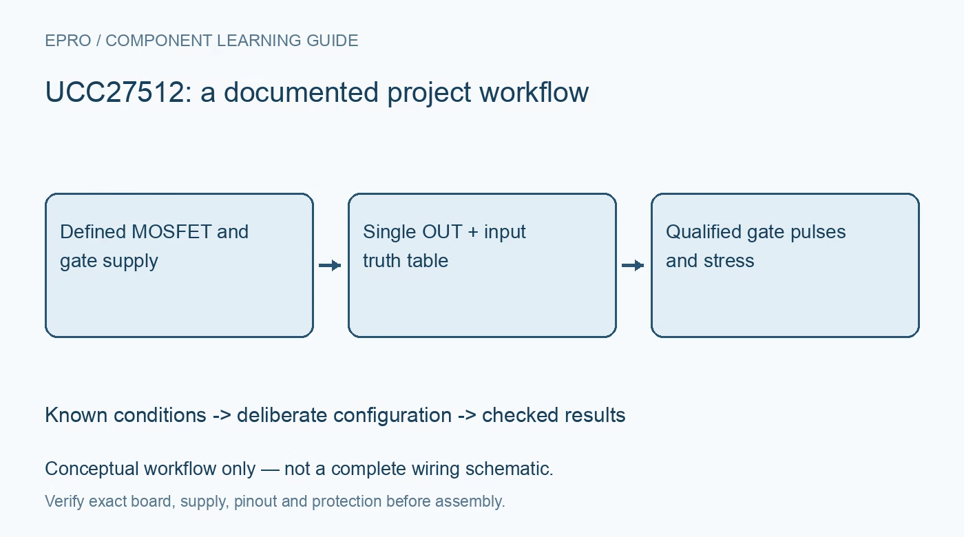
UCC27512 Gate Driver: 7 Checks for Its Single Output
Check UCC27512 single-output pin mapping, dual-input logic, supply headroom and gate-loop stress before switching a MOSFET. This is a documentation-based planning guide, not a report of independent hands-on testing.
1. Distinguish UCC27512 from the split-output device
The UCC2751x family datasheet describes related devices with different output arrangements. UCC27512 has one OUT terminal; the separate OUTH and OUTL arrangement belongs to UCC27511. Confirm the exact marking and package before transferring a schematic. In the six-pin UCC27512 pinout, OUT is pin four, with ground connections on pins two and five. A family resemblance does not make those terminals interchangeable with a split-source-and-sink gate-drive network. Manufacturer documentation.
2. Translate both inputs into an explicit truth table
UCC27512 has IN+ and IN− rather than an independent conventional enable pin. Its output goes high when IN+ is high and IN− is low. Decide whether the controller needs noninverting or inverting operation, then bias the other input deliberately according to the documentation. Include controller reset and disconnected-controller states in the table. Internal input biasing helps establish a low output, but deliberate external signal planning is preferable to relying on an unknown board pull resistor. Manufacturer documentation.
3. Match the driver rail to the transistor gate rating
The recommended driver supply range is 4.5 V to 18 V, and the high output follows that driver rail rather than becoming a regulated logic voltage. Check the MOSFET gate-source maximum, intended enhancement voltage and any gate protection. A controller with low-voltage logic does not limit the gate-drive amplitude. Verify VDD at the driver pins during startup and switching, including droop and overshoot, before connecting a power stage that can deliver substantial fault energy. Manufacturer documentation.
4. Use peak current ratings for switching analysis
The advertised four-ampere source and eight-ampere sink capabilities describe peak gate-drive behavior, not continuous output load ratings. Estimate the required gate charge per transition and average switching demand, then consider pulse current, external gate resistance and thermal dissipation. Since this part has a single output, independently adjusted turn-on and turn-off paths require an appropriate external network rather than separate driver output pins. Choose component pulse ratings and voltage margins for that network, not just nominal resistance. Manufacturer documentation.
Newest in the store


5. Keep the complete gate-current loop compact
Place the local bypass capacitor near VDD and the driver grounds so that charging current does not traverse a long shared logic return. Route OUT to the gate with a short return path to the transistor source reference. Include package connections, gate resistance and measurement probe inductance when assessing ringing. A neat signal trace alone is insufficient if the return loop is large. Follow the manufacturer layout guidance before attempting to solve parasitic oscillation entirely through firmware timing. Manufacturer documentation.
6. Check undervoltage and restart without assuming interlock
The undervoltage-lockout function holds the output low when the supply is not adequate for normal operation. That protection does not provide galvanic isolation, high-side level shifting or coordination between two power switches. If the application uses a half bridge, dead time and shoot-through prevention require a system-level design. Check both input states as the driver rail crosses its operating region. Confirm that a controller restart cannot create an unintended high pulse when VDD recovers. Manufacturer documentation.
7. Validate gate pulses before enabling power transfer
Begin with a current-limited driver supply and a safe test arrangement that represents the intended gate load. Observe gate-source voltage at the transistor, not only OUT relative to a distant ground. Check amplitude, edge behavior and the response to disabled inputs across the intended operating conditions. Move to an energized power stage only after its independent protection is established. No switching waveforms or efficiency figures in this guide are presented as hands-on results; retain measured observations separately from datasheet expectations. Manufacturer documentation.
Related reading: UCC27511 Gate Driver: 7 Checks Before Connecting a Power Stage.
Catalog note: The exact-part search did not return a matching Epro listing during preparation. Check the current catalog; this guide makes no price, availability or included-accessory claim.