


CD4051 Analog Multiplexer: 7 Rail and Loading Checks

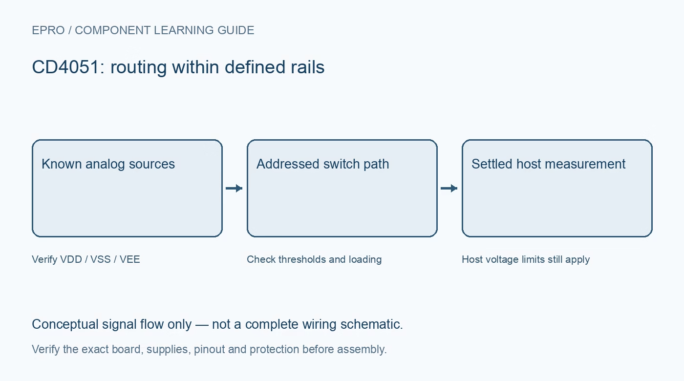
A CD4051B connects one of eight analog channels to a common terminal. It routes a signal but does not convert it to digital data or guarantee compatibility with a host ADC. Read the exact manufacturer variant and plan the full signal path before selecting a module.
Identify the exact family and package
This guide uses the TI CD4051B documentation, not every device with 4051 in its name. HC and other family versions can differ in supply range, thresholds and resistance. Check package orientation and carrier labels rather than applying a remembered pin drawing to an unidentified board.
Understand VDD, VSS and VEE
The control logic is referenced to VSS and VDD, while the permitted analog path extends between VEE and VDD. In an appropriate single-supply arrangement VEE is tied to the low rail, not left floating. Dual-supply operation needs a deliberate complete design, not a guessed negative connection.
Keep the host measurement limits separate
A switch capable of routing a negative or larger analog signal does not make that signal safe for an ordinary microcontroller ADC. Protect or condition the destination independently. The phrase logic-level conversion in the part description is not a guarantee of automatic ADC voltage scaling.
Check control-input thresholds at the chosen supply
Address and inhibit signals must meet the manufacturer’s specified high and low levels. A 3.3 V microcontroller is not automatically a valid controller for every higher-voltage CD4051B configuration. Select compatible rails or a properly designed interface rather than relying on an apparently working room-temperature example.
Include switch resistance and loading
ON resistance varies with supply and signal conditions, and the common terminal is not a buffered low-impedance output. A load can create voltage error through the selected switch. Evaluate source impedance, leakage and acquisition capacitance before treating the routed voltage as an ideal copy.
Allow settling after a channel change
Address propagation is only one part of the delay. The sensor, wiring and ADC sampling network also need time to settle after selection. High-impedance sources can show previous-channel memory, so choose buffering or an adequate acquisition schedule for the required measurement accuracy.
Newest in the store


Keep the initial application low risk
Use known low-voltage signals with a suitable high-impedance measurement input. Inhibit high disconnects the channels but does not ground the common terminal. Do not switch mains, motors, relay coils or substantial power through the device, and do not treat a disabled path as safety isolation.
Frequently asked questions
Can VEE simply be left unconnected on a single supply?
No. Use the defined supply connection specified for the intended single-supply arrangement.
Does the multiplexer convert a selected signal into an ADC-safe voltage?
No. The destination’s voltage limits and any required conditioning remain separate design responsibilities.
Availability and illustration note
No matching Epro product was returned by the catalog search on 21 October 2026 UTC. This learning guide does not assert stock, a selling price or compatibility of an unidentified substitute. The illustration is an original conceptual signal-flow diagram, not a product photograph or complete wiring schematic.
Related Epro reading
For a first bench setup, review breadboard connections and continuity checks and I2C voltage-level translation. These guides do not replace the exact module schematic.
Technical references and limitations
Source: Texas Instruments CD4051B/CD405xB datasheet. Electrical limits apply to the named part, not automatically to every carrier board. This is a documentation-based learning workflow, not a claim of independent hardware testing, traceable calibration or safety certification.