


MCP3424 ADC: 7 Resolution and Differential Checks

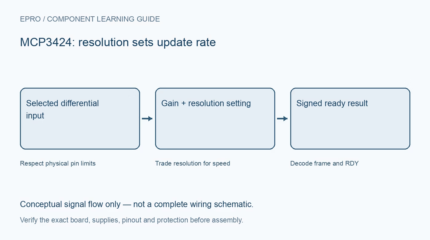
An MCP3424 provides four multiplexed differential channels with a built-in reference and selectable resolution. The most detailed output is also its slowest conversion setting. Match that trade-off to the actual signal and update requirement before selecting a module for a low-voltage monitoring experiment.
Inspect the exact carrier and supplies
The chip operates from a 2.7 V to 5.5 V supply, but a carrier can add pull-ups and address straps that change host compatibility. Verify the schematic and fitted components. A voltage marking on a power connector does not establish the allowable voltage on every host data pin.
Choose resolution together with rate
The documented settings are twelve bits at 240 samples per second, fourteen at 60, sixteen at 15 and eighteen at 3.75. These are not simultaneously available headline features. Include conversion time and host polling overhead when deciding whether the slow eighteen-bit setting suits a changing signal.
Remember that inputs are multiplexed
Four differential channel pairs feed a shared converter. They do not deliver four simultaneous samples. A scanning design must allow a completed conversion for the selected channel and preserve the channel label with each result. Phase-sensitive multi-channel measurements need a different timing analysis or architecture.
Separate differential span from pin limits
The nominal span is plus or minus 2.048 V divided by the selected PGA gain. Both physical inputs must still remain within their allowed absolute voltages. A negative differential code can result from two positive inputs with the negative terminal higher; it does not authorize driving a pin below ground.
Use reference and gain honestly
The internal reference simplifies the circuit, and PGA gains of one, two, four and eight change the input scale. Neither eliminates wiring, noise, offset or source errors. Internal calibration features are not a traceable calibration of the assembled sensor, input network and measurement environment.
Plan address straps and pull-ups
Read the address-configuration table for the exact carrier and its external address pins. Do not guess the address from a different board photograph. Verify I2C pull-ups terminate at a compatible rail and that parallel boards do not produce an excessively strong combined pull-up or duplicate addresses.
Newest in the store


Define what a useful result means
At eighteen bits and unity gain the ideal voltage step is 15.625 microvolts; higher gain reduces that step further. Such a small code increment is not guaranteed absolute accuracy. Document conversion mode, rate, gain and sample age, and test with protected known low-voltage sources before attaching a sensor.
Frequently asked questions
Can MCP3424 deliver eighteen-bit readings at 240 SPS?
No. The documented resolution and rate settings are linked; 240 SPS is the twelve-bit setting.
Does differential input mean isolated input?
No. Both terminals remain constrained by the converter supply and input specifications.
Availability and illustration note
No matching Epro product was returned by the catalog search on 21 October 2026 UTC. This learning guide does not assert stock, a selling price or compatibility of an unidentified substitute. The illustration is an original conceptual signal-flow diagram, not a product photograph or complete wiring schematic.
Related Epro reading
For a first bench setup, review breadboard connections and continuity checks and I2C voltage-level translation. These guides do not replace the exact module schematic.
Technical references and limitations
Source: Microchip MCP3422/3423/3424 datasheet. Electrical limits apply to the named part, not automatically to every carrier board. This is a documentation-based learning workflow, not a claim of independent hardware testing, traceable calibration or safety certification.